
Apple Files Patent for a Tighter Dot Layout That Captures More Depth Detail
Apple's latest optics filing swaps the square grid of microscopic pillars that splits laser light for a honeycomb grid. The result is about 15% more pillars in the same space, and more of the light lands where it's supposed to.
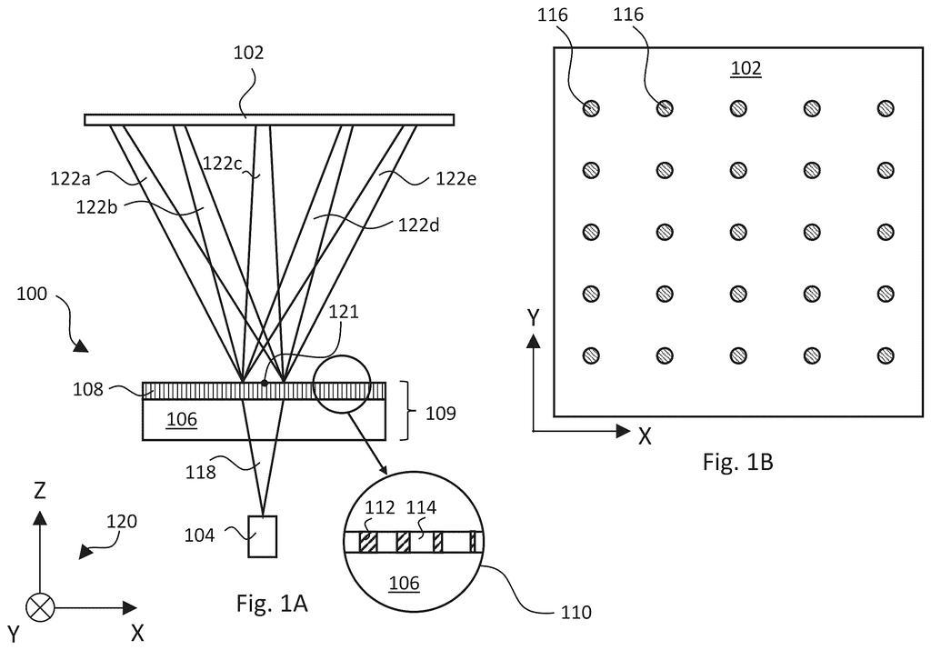
What Apple's honeycomb light-splitter does
Every time a phone or headset maps the room in front of it, it fires out a grid of tiny invisible dots and watches how they land. Those dots start as a single laser beam that has to be split into many, and any light that strays off course is wasted.
The splitting is done by a flat, thin layer covered in microscopic pillars, each smaller than a wavelength of the light itself. Apple's filing arranges those pillars in a honeycomb pattern instead of the usual square grid. A honeycomb fits about 15% more pillars into the same space, and more pillars means more of the light ends up in the dots you actually want.
The pillars still vary in width in a repeating pattern, so the dots still come out as a neat rectangular grid. Only the layout underneath changes.
… an array of pillars, which are arranged in a hexagonal lattice having a pitch no greater than half the target wavelength, and have varying respective diameters that are chosen to define a periodic pattern over a plane of the substrate having a unit cell larger than the target wavelength.
Translation: Tiny pillars are packed tightly together in a specific honeycomb pattern to bend light in precise ways.
How hexagon-packed pillars split one laser beam
The device is a piece of glass (the substrate) topped with a metasurface, a thin layer of pillars that bend light. How wide each pillar is sets how much it delays the light passing through, and the right pattern of delays can split one beam into many.
The claims cover pillars sitting in a hexagonal lattice (a honeycomb arrangement) with a spacing no greater than half the light's wavelength. The pillar widths repeat in a tile, called a unit cell, that is larger than the wavelength. The tile can be a hexagon, a parallelogram or a rectangle. In one example, an 8 by 8 tile about 3 micrometers across splits a beam into a 5 by 5 fan, and 20 by 20 of those tiles make a 60 micrometer square element.
The filing also describes layering a second, non-repeating pattern on top, such as a quadratic (bowl-shaped) phase, so the same surface can focus or straighten the split beams. Other claims cover a version with laser emitters attached and a method for making the layer.
For the numbers, the description says a honeycomb is 15% denser than a square grid at the same spacing. In computed tests, efficiency rose by more than 14% at very steep bending angles, and by about half that at 45 degrees.
What denser pillars could mean for Apple sensors
If you own a phone, headset or smart glasses that scans the space around you in 3D, the light source inside is small and has a limited power budget. A layer that wastes less light means the same laser can do more, which could help with battery life or sensor range. The filing doesn't promise either, but it's the direction the efficiency numbers point.
The design also stays within standard chip-style manufacturing, with spacing the filing calls readily achievable (380 to 470 nanometers) for 940 nm infrared light. That keeps the idea practical, since it only changes where the pillars go.
This is the 60th Apple filing we've tracked since May in the AR glasses race, joining earlier applications on brightening lenses with overlapping patterns and frame bending detection.
You will never see this change, and that's the point. The benefit shows up as a 3D sensor that wastes less of its own light, which could translate into a slightly longer-lasting battery or a dot pattern that stays usable a bit farther out.
The gain is modest and the filing says so: a 15% denser layout, and efficiency up by roughly 14% at the most extreme bending angles. At the more moderate angles it's about half of that. Those are computed results, not measurements from a built device.
Still, it's a tidy trick. Changing only the layout, with no new materials or manufacturing steps, is the easiest kind of upgrade for a device maker to adopt, and it could make face and room scanning a little more efficient.
Get our take in your Top Stories
Liked this breakdown? Add Patentlyze as a preferred source on Google, and our plain-English take shows up more often in your Top Stories the next time Apple patent news breaks.
There are more where this came from
We read every patent application Big Tech publishes and send you the ones worth knowing. Plain English, free, every week.
The drawings
16 drawing sheets from US 2026/0339005 A1 · click any drawing to enlarge


Show the other 8 sheets


Want this weekly breakdown for a company we don't cover? Patentlyze Pro →
Be the first to weigh in