Samsung Patent Details Display Wear Data Compression Method to Reduce Memory Usage
Every pixel on an OLED screen gradually wears out, and Samsung's displays already track that wear. This patent is about squeezing all that tracking data into a much smaller slice of memory.
What Samsung's pixel stress tracking system actually does
Imagine your phone's screen is secretly keeping a log of how hard each of its millions of tiny pixels has been working. Bright pixels that stay on for hours age faster than dim ones, so tracking that wear helps the display compensate and stay looking even. The problem is that log takes up a lot of memory.
Samsung's patent describes a way to compress that wear-tracking data before storing it. The system looks at a batch of pixel stress readings, finds a value that represents the whole group well, adjusts each individual reading relative to that shared anchor, and then encodes everything in a more compact form.
The end result is that your display's internal bookkeeping takes up less working memory, which frees that memory for other tasks and could make the whole process cheaper to build into a chip.
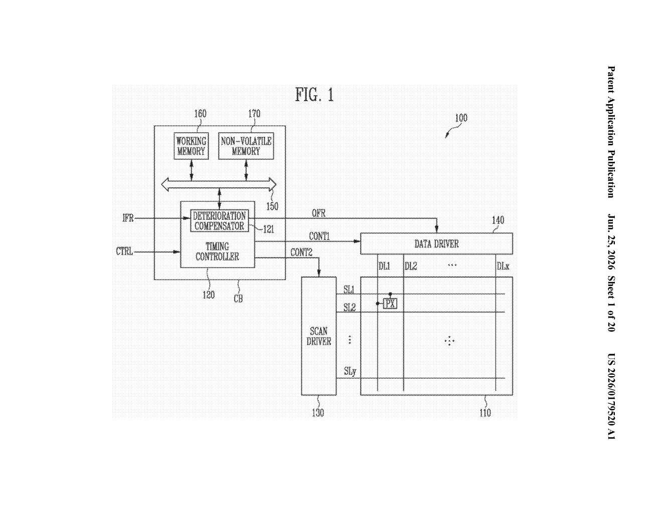
How the controller compresses accumulated stress data
The patent covers a display device with three main parts: a display panel (the screen itself), a controller (the chip managing the panel), and working memory (fast, temporary storage the controller reads and writes constantly).
The controller runs a four-step loop:
- It updates accumulated stress data for every pixel based on recent image frames, essentially tallying up how much wear each pixel has taken on.
- It groups those stress readings into source data units and calculates a representative value for each group, a kind of average anchor for the cluster.
- It rewrites a portion of the data bits in each unit relative to that anchor, so instead of storing large absolute numbers, it stores smaller relative differences.
- It then encodes the adjusted values into compressed data and writes that to working memory.
This is a form of delta or reference-based compression (storing differences from a shared baseline rather than full values), a common technique in video and sensor data, applied here to pixel-aging information.
What this means for display longevity and memory efficiency
OLED screens dim and shift color unevenly over time, and display makers use pixel-level compensation circuits to fight that. Those circuits need a running record of wear per pixel, which on a high-resolution panel adds up to a significant amount of data written and read constantly during normal use. If that data can be compressed efficiently, the working memory required gets smaller, the controller's memory bus is less congested, and the feature becomes cheaper to implement in lower-cost devices.
For you as a user, the practical upshot is that display compensation tech could eventually appear in more affordable screens without sacrificing picture quality or longevity. This patent sits in the engineering plumbing of that goal rather than in any visible feature.
This is unglamorous but genuinely useful display engineering. Pixel-level stress compensation is already in high-end Samsung panels; the interesting work here is making the memory overhead of that system smaller so it can scale down-market. Worth a note if you follow display technology or memory architecture, easy to skip otherwise.
Get one Big Tech patent every Sunday
Plain English, intelligent commentary, no hype. Free.
Editorial commentary on a publicly published patent application. Not legal advice.