AMD Patents a Dedicated Chip Core Built to Make Images Sharper with AI
AMD is patenting a dedicated slice of silicon — a purpose-built processing core — whose entire job is to handle the math behind AI-powered image upscaling. That's a notable architectural shift from how AMD handles this today.
What AMD's dedicated upscaling core actually does
Imagine your GPU is like a restaurant kitchen. Right now, AMD's kitchen uses the same general-purpose cooks for everything — frying, plating, and now also running the AI that makes blurry images look sharp. This patent describes adding a specialist to the team: a dedicated station whose only job is that AI sharpening work.
The specific technique is called image super resolution — it's what lets games and video apps take a lower-resolution image and reconstruct a higher-quality version using a neural network. AMD already offers this with its FSR (FidelityFX Super Resolution) technology, but currently it runs on the same general compute units everything else uses.
This patent describes carving out a dedicated core just for the convolution math that powers super resolution. The idea: let the specialist handle that one task so the rest of the GPU stays free for rendering the game itself.
How the convolution core feeds AMD's SIMD pipeline
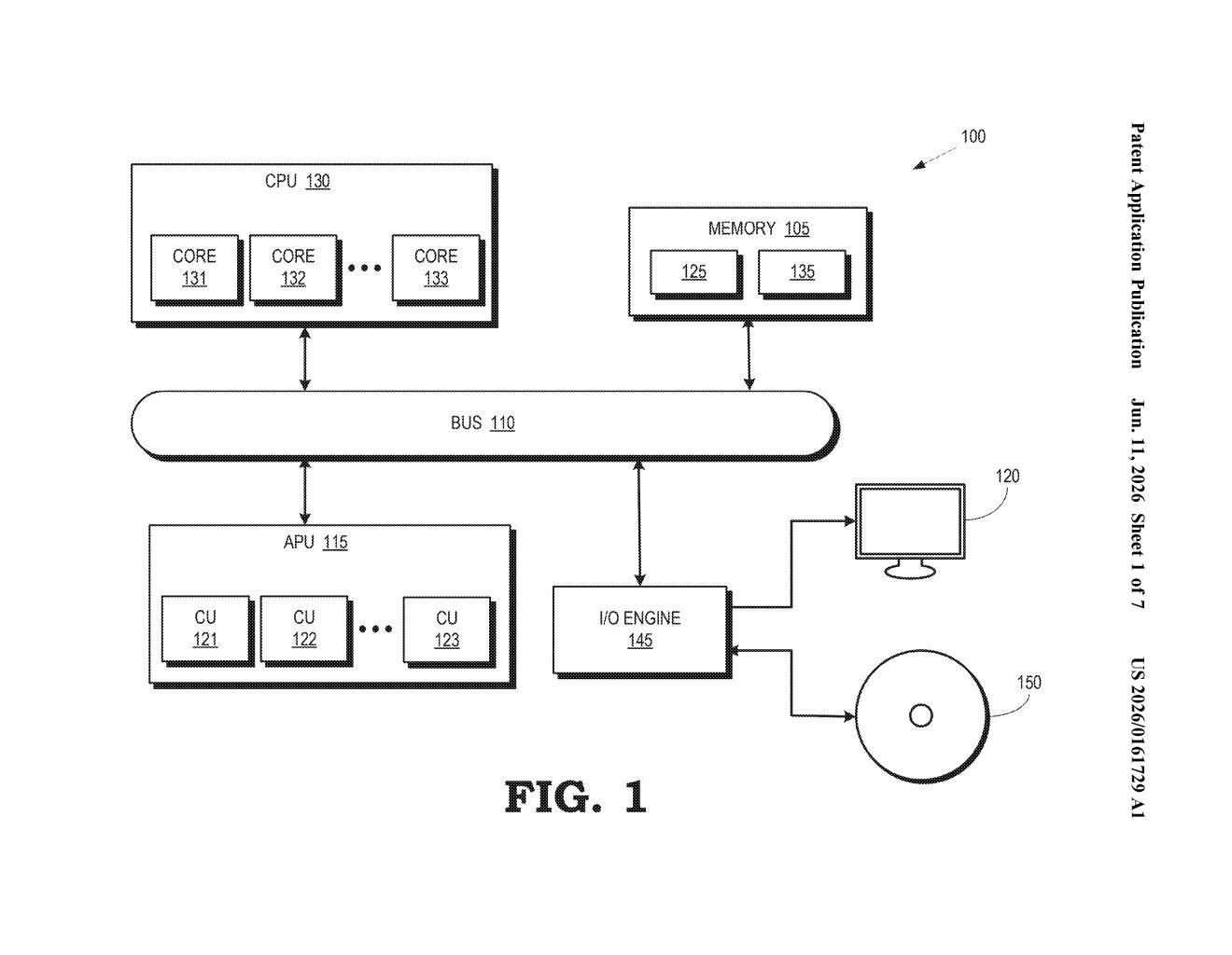
The patent describes an accelerated processing unit (APU or GPU) that includes a new hardware block called a convolution core — a fixed-function circuit dedicated to running convolution operations.
Convolution (think of it as a sliding filter that scans across an image and detects patterns like edges or textures) is the fundamental math operation inside most image-processing neural networks. Today, AMD's GPU handles convolutions using its general-purpose SIMD units (Single Instruction, Multiple Data — processors that apply the same operation to many data points at once, in parallel).
In the patented design, the convolution core sits upstream of the SIMD units:
- It fetches raw image data from memory.
- It runs the convolution operations independently, producing pre-processed output called convolved data.
- It hands that convolved data off to the SIMD units, which then handle the remaining neural-network steps — activation functions, normalization, and final pixel reconstruction.
By separating the convolution workload into its own pipeline, the chip can potentially run both stages in parallel rather than sequentially, reducing how long super resolution takes to complete each frame.
What this means for AMD's rivalry with Nvidia DLSS
Nvidia has had dedicated hardware for AI upscaling — its Tensor Cores — since 2018, and DLSS (Deep Learning Super Sampling) has been a consistent marketing and performance advantage. AMD's FSR has historically run on standard shader cores, which is one reason FSR is more hardware-agnostic but also potentially less efficient per watt. A dedicated convolution core would be AMD's most direct architectural answer to that gap.
For you as a gamer or creative professional, this kind of silicon efficiency matters because it can mean higher frame rates with AI upscaling active, or the same frame rates at lower power draw. It also signals that AMD sees AI-driven image processing as important enough to bake permanently into its chip architecture — not just run as software on top of existing cores.
This is a genuinely interesting patent because it signals AMD may be planning to close one of the most concrete hardware gaps between its GPUs and Nvidia's. Dedicated fixed-function silicon for AI upscaling is exactly the kind of long-term architectural commitment that separates a feature from a roadmap priority. Whether AMD's implementation can match Tensor Core efficiency remains to be seen, but the direction is clear.
Get one Big Tech patent every Sunday
Plain English, intelligent commentary, no hype. Free.
Editorial commentary on a publicly published patent application. Not legal advice.