
Samsung Patents an Under-Display Fingerprint Sensor Built Into the Pixel Layer
Samsung's new patent tucks a capacitive fingerprint sensor directly into the same layer as the display's pixel electrodes — no separate sensor module needed, no extra thickness.
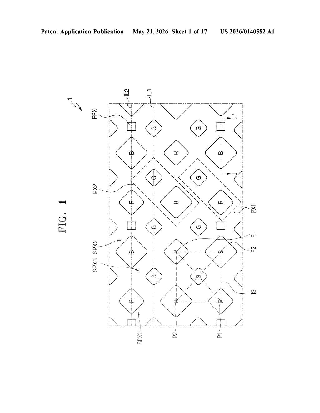
How Samsung hides a fingerprint sensor inside the display stack
Imagine pressing your finger on a phone screen to unlock it. Most current under-display fingerprint sensors are optical — they use a camera-like component sitting beneath the screen to catch light bouncing off your fingerprint ridges. That approach works, but it adds bulk and complexity.
Samsung's patent describes a different approach: placing a capacitive sensing electrode — the kind that detects the tiny electrical differences between your fingerprint's ridges and valleys — on the same physical layer as the pixels themselves. Your finger changes the capacitance (think of it like a tiny electrical field) when it touches the screen above that electrode, and the sensing circuit reads those changes to identify your print.
The clever part is what happens in the OLED layer directly above. Samsung cuts a deliberate gap — an opening in the facing electrode of the display — right over the fingerprint sensor area, so the sensor can actually do its job without the display's own electrical layer interfering. It's a tight bit of engineering that could make future displays thinner and simpler.
How the shared electrode layer and OLED opening work together
The patent describes a display apparatus — almost certainly an OLED panel — where a capacitive fingerprint sensor is co-planar with the light-emitting pixels rather than stacked underneath them as a separate module.
The key structural move: the first electrode (the sensing electrode) and the pixel electrode of an OLED pixel sit on the same layer and are simply spaced apart from each other. Normally these would be separate physical layers with their own fabrication steps. Combining them reduces stack height and simplifies manufacturing.
Above both electrodes sits the OLED's facing electrode (typically a shared cathode layer covering the whole display). The patent specifies that this facing electrode has an opening — a deliberate gap — that overlaps the sensing electrode in plan view (meaning if you looked straight down through the display). This gap prevents the conductive cathode from shorting out or masking the capacitive signal the sensor is trying to read from your fingertip.
The sensing circuit itself is described as being arranged around the pixel circuits of a neighboring pixel group — tucked into the unused space in the pixel layout rather than requiring its own dedicated real estate. The result is a sensor that is, in theory, more tightly integrated and potentially manufacturable on existing OLED production lines.
What this means for thinner, cleaner display designs
Under-display fingerprint sensors are already common on Android flagships, but most rely on optical methods that require a bright flash and a camera module below the panel. Capacitive under-display sensors are faster and work in more lighting conditions, but fitting them into an OLED stack without sacrificing display quality or adding thickness has been the engineering challenge. This patent is Samsung Display's take on solving that at the fabrication level.
For you as a user, the downstream payoff could be a phone or tablet that unlocks faster and more reliably — and potentially a display that's thinner because it doesn't need a separate optical sensor module. Given that Samsung Display supplies panels to a wide range of device makers beyond Samsung Electronics itself, a manufacturable version of this design could show up in many places.
This is solid, incremental display engineering — not a dramatic leap, but exactly the kind of fabrication-level work that determines whether a feature ships at scale or stays a prototype. The co-planar electrode approach is a real structural insight, and the opening-in-the-cathode trick is the kind of detail that separates a patent with actual implementation thinking from a purely speculative filing. Worth tracking as a signal that Samsung Display is serious about capacitive under-display sensing.
Get our take in your Top Stories
Liked this breakdown? Add Patentlyze as a preferred source on Google, and our plain-English take shows up more often in your Top Stories the next time Samsung patent news breaks.
There are more where this came from
We read every patent application Big Tech publishes and send you the ones worth knowing. Plain English, free, every week.
Want this weekly breakdown for a company we don't cover? Patentlyze Pro →