Samsung Display Patents a Per-Zone Voltage Tuning Method for Uneven-Density Screens
Screens with under-display cameras have a dirty secret: the area above the camera uses a sparser pixel grid, and that mismatch can make brightness uneven. Samsung Display's new patent tackles that inconsistency at the voltage level.
What Samsung's pixel-density voltage trick actually does
Imagine looking at your phone's screen and noticing a faint bright or dim circle right above the front camera — a subtle reminder that the pixels there are packed differently than the rest of the display. That's the kind of visual artifact Samsung Display is trying to eliminate with this patent.
The idea is to assign different low driving voltages (the minimum power each pixel zone needs to light up properly) to different parts of the screen based on how densely packed the pixels are. A denser zone and a sparser zone need different voltages to hit the same perceived brightness.
To make sure those voltages are actually right, the system runs an optical correction check at maximum brightness for each reference brightness level, then automatically adjusts the voltage up or down if the result isn't accurate. It's essentially a self-calibration routine baked into the display's setup process.
How the optical correction loop adjusts each voltage zone
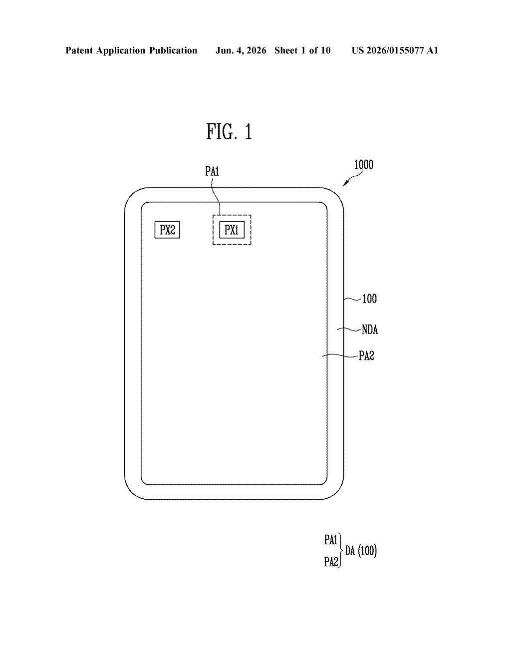
The patent describes a calibration method for a display that contains at least two pixel areas: a first pixel area with a standard pixel density and a second pixel area with a higher pixel density (think the ring of pixels directly over an under-display camera versus the rest of the panel).
The process works in three steps:
- Set reference voltages: A table of low driving voltages (ELVSS or similar — the supply rail that sets the floor voltage for OLED pixels) is established, one voltage per reference brightness level.
- Run optical correction: For a given reference brightness, the system drives the display at maximum grayscale using the assigned low driving voltage and measures the optical output — essentially asking 'does this voltage actually produce the right brightness?'
- Selectively update the voltage: If the measured output is off, the low driving voltage for that brightness level is changed. If it's within tolerance, it stays put.
The 'selective' part is important: the method doesn't blindly recalibrate everything — it only changes a voltage when the optical test proves it's wrong. This keeps the calibration efficient and avoids over-correcting zones that are already accurate.
What this means for under-display camera screen quality
Under-display camera displays are now common in foldables and are showing up in more flagship phones. The zone above the camera always has a lower pixel density, which means it draws current differently — and without per-zone voltage calibration, you get visible brightness non-uniformity that no amount of software color correction fully fixes.
This patent suggests Samsung Display is investing in hardware-level calibration routines that run at the voltage supply layer, not just the pixel data layer. For consumers, that means displays where the under-camera region is less visible in everyday use. For Samsung's display business, it's the kind of manufacturing and tuning IP that keeps panel quality ahead of competitors shipping similar form factors.
This is unglamorous but genuinely useful engineering. Under-display camera panels are a known weak spot for display quality, and addressing it at the driving-voltage level rather than papering over it with image processing is the right approach. It's not a headline feature, but it's exactly the kind of detail that separates a great panel from a merely good one.
Get one Big Tech patent every Sunday
Plain English, intelligent commentary, no hype. Free.
Editorial commentary on a publicly published patent application. Not legal advice.