Samsung Patents a Two-Layer Shield for Stacked Camera Sensor Chips
Modern smartphone camera sensors are built from multiple chips stacked on top of each other — and the tiny electrical pins connecting those layers are a vulnerability. Samsung's latest patent describes a double-layer armor system designed to keep those connections intact.
What Samsung's stacked image sensor protection actually does
Imagine your smartphone camera sensor as a skyscraper with two floors. The top floor captures light; the bottom floor processes it. To move data between them, engineers drill tiny electrical tunnels — called vias — straight through the floors. Those tunnels are fragile, and if they crack or get contaminated during manufacturing, your camera fails.
Samsung's patent describes a way to protect those tunnels using two stacked protective layers. The first layer sits directly over the tunnels and forms individual caps — one or more caps per tunnel — like little helmets. The second layer covers the entire sensor surface, including the light-focusing microlenses, and adds another set of bumps lined up exactly over the first ones.
The result is a double-reinforced zone around every tunnel, reducing the chance that mechanical stress or manufacturing imperfections cause failures where the two chips meet.
How the two protective layers guard the through-chip connectors
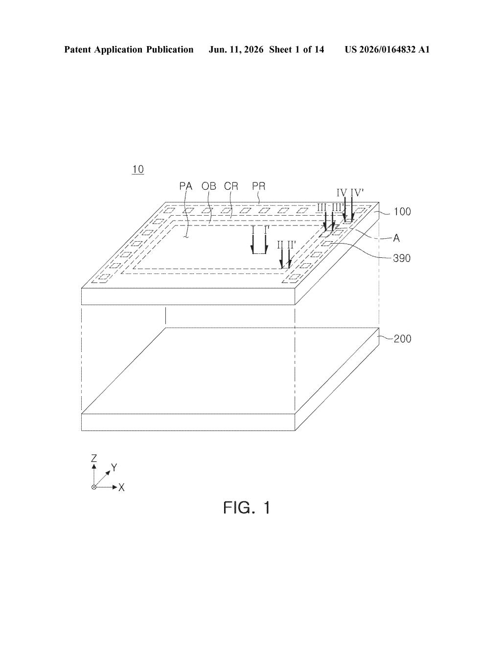
The patent describes a stacked image sensor made of two chips bonded together. The top chip (the first chip) contains the pixel array — the grid of light-sensing cells — along with a pad region for external connections and an inter-chip connection region in between, where electrical tunnels (called through-via structures) punch all the way through the first chip and into the second chip below.
The innovation is a two-layer protective structure sitting above those vias:
- A first protective layer is placed over the inter-chip connection region and forms individual raised patterns — one per via or per small group of vias — directly on top of each tunnel.
- A second protective layer is then spread across the entire top surface of the sensor, covering both the microlenses (the tiny curved lenses that focus light onto each pixel) and the first protective layer. Crucially, this second layer forms its own raised patterns aligned precisely on top of the first layer's patterns.
The stacked, aligned bumps create a localized stress-relief zone. When the chip package flexes, expands with heat, or undergoes pressure during assembly, the double-pattern geometry helps absorb and distribute mechanical forces away from the electrically critical via structures beneath.
What this means for camera reliability in future Samsung devices
Stacked image sensors — where a dedicated processing chip sits directly below the pixel chip — are now standard in flagship smartphones and increasingly common in automotive and surveillance cameras. The via connections between the two chips are among the most failure-prone points in the entire assembly, especially as sensors shrink and chip stacks get taller.
A more reliable inter-chip connection means fewer defective sensors coming off the production line and longer-lasting cameras in your hands. For Samsung, which supplies image sensors to its own Galaxy phones and to third-party device makers, even small improvements in manufacturing yield translate into meaningful cost savings and a quality advantage over competitors.
This is a focused, incremental manufacturing patent — not a sensor capability leap. It addresses a real engineering problem (protecting stacked-chip vias from mechanical stress) and the dual-pattern approach is a clean solution. It matters most to Samsung's manufacturing teams and camera reliability engineers, less so to consumers who will never know it exists.
Get one Big Tech patent every Sunday
Plain English, intelligent commentary, no hype. Free.
Editorial commentary on a publicly published patent application. Not legal advice.