
Samsung's New Patent Stops AI Memory Chips from Cracking During Assembly
Samsung has patented a memory chip stack with a specially shaped cap layer designed to keep the whole structure from cracking or warping during manufacturing. It's a packaging tweak, but in the world of high-bandwidth memory, small structural changes can have big consequences for reliability.
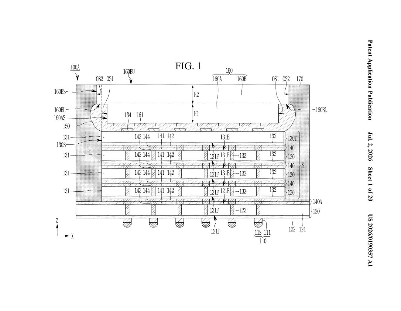
What Samsung's stepped dummy die actually does
Imagine stacking a dozen thin crackers on top of each other, then covering the whole pile in a protective resin. If the top cracker is the same size as all the others, the resin can pull unevenly as it hardens and crack the stack. Samsung's patent describes a smarter way to handle that top layer.
Instead of a plain flat chip on top, Samsung wants to use a dummy die (a non-functional chip whose only job is structural) that is shaped like a stepped platform. The bottom part of it is narrower than the memory chips below, and the top part flares back out to full width or wider. That notched shape gives the surrounding protective resin something to grip onto more evenly.
This kind of work sits deep inside chip manufacturing, invisible to end users. But high-bandwidth memory is the type of RAM packed into AI accelerators and graphics cards, so anything that improves its yield or durability ultimately matters to anyone buying hardware that runs AI workloads.
How the notched cap die fits into the memory stack
The patent describes a high-bandwidth memory (HBM) module built as a vertical stack of chips. At the bottom sits a base die that handles input/output. Above it are several core dies (the actual memory layers), all sharing the same horizontal width.
On top of the memory stack, Samsung places a dummy die with an unusual two-part shape:
- A first portion (the bottom half of the cap) that is narrower than the memory dies below it
- A second portion (the top half) that is equal to or wider than the memory dies
Between the dummy die and the top memory die sits an insulating layer to prevent unintended electrical contact. The entire assembly is then encased in a molding material that wraps around all the side surfaces.
The stepped shape of the dummy die creates a mechanical interlock with the molding compound. When the resin shrinks as it cures, the wider top ledge of the dummy die resists delamination and helps distribute stress more evenly across the stack. This is a packaging engineering solution aimed at reducing warpage and improving manufacturing yield rather than adding new electrical capability.
What this means for AI chip memory packaging
High-bandwidth memory is the critical component inside Nvidia's H100 and similar AI accelerators, where dozens of chips are stacked and bonded in tight proximity. Failures during the molding and curing process are one of the main reasons finished HBM modules get rejected, and those rejections drive up cost for everyone downstream.
A structural improvement at this layer could let Samsung improve yield on its HBM production lines, which matters a lot given how tight supply has been. For you as a consumer or enterprise buyer, better yields on HBM packaging translate to lower prices and more available supply for the AI hardware that's currently in short supply.
This is unglamorous but genuinely useful work. HBM packaging reliability is a real production bottleneck right now, and a structural fix that costs nothing in extra material or process steps is exactly the kind of incremental win that separates high-yield fabs from low-yield ones. It won't make headlines outside the semiconductor industry, but it's the kind of patent that earns its keep on a factory floor.
Get our take in your Top Stories
Liked this breakdown? Add Patentlyze as a preferred source on Google, and our plain-English take shows up more often in your Top Stories the next time Samsung patent news breaks.
There are more where this came from
We read every patent application Big Tech publishes and send you the ones worth knowing. Plain English, free, every week.
Want this weekly breakdown for a company we don't cover? Patentlyze Pro →