
Samsung Files Patent for a Display That Senses Light Without Extra Sensors
Samsung Display is patenting a screen that doubles as a light sensor — embedding light-receiving elements directly into the panel and using a clever spatial trick to get clean readings without cross-talk from neighboring pixel groups.
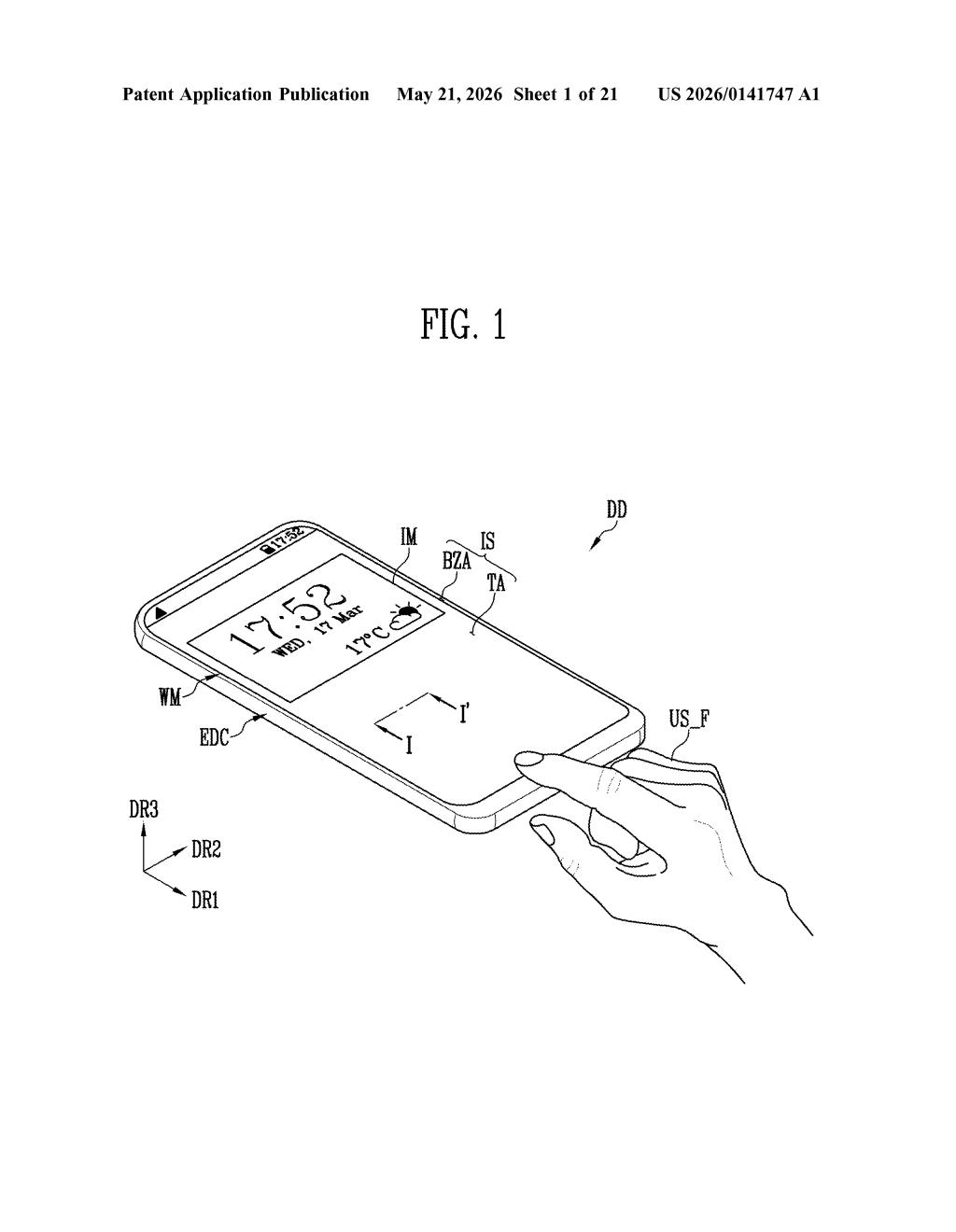
What Samsung's light-sensing display panel actually does
Imagine your phone's screen could sense what's in front of it — your finger, your face, ambient light levels — without any dedicated sensor cutout or under-display camera module. That's the direction Samsung is pointing here.
The patent describes a display panel where light-receiving elements (basically tiny photodetectors) sit right alongside the light-emitting elements (the pixels you normally see). The tricky part is keeping those sensors from getting fooled by the glow of their nearest neighbor pixels. Samsung's answer: when one group of pixels lights up, you read the sensor data from a group that's farther away, not the one sitting right next to it.
It's a bit like taking a photo of something bright by looking slightly to the side rather than directly at it — you avoid the glare. The result is cleaner sensing data baked right into the display surface, with no extra hardware punching holes in the screen.
How the emit-and-skip sensing geometry works
The patent describes a display panel with two interleaved populations of elements on the same substrate: light emitting element groups (LEGs) arranged in rows along one axis, and light receiving element groups (LRGs) running parallel to them.
The sensing logic is the interesting part. When a first LEG fires, the system deliberately skips the LRG that's physically closest to it — because that nearby sensor would be overwhelmed by direct light from those pixels. Instead, the system reads from an LRG that sits adjacent to a different, currently-off LEG farther along the panel.
- LEGs all emit the same color of light, keeping the optical environment consistent for sensing
- LRG columns are interleaved with LEG columns along the same first direction
- The "skip the nearest sensor" rule reduces optical crosstalk (signal contamination from adjacent emitters)
- Sensing data is composited from the spatially offset LRGs to reconstruct what's in front of the screen
This is essentially a structured-light sensing approach — emit from one location, read from another offset location — implemented entirely within the flat panel stack rather than relying on a separate sensor layer or module.
What this means for under-display biometrics and sensing
Under-display sensing is one of the harder unsolved problems in display engineering. Current solutions — under-display fingerprint readers, under-display cameras — require optical compromises or dedicated cutouts. Integrating light-receiving elements directly into the emissive layer, and solving the crosstalk problem with a spatial offset trick rather than extra shielding hardware, could allow thinner devices with larger usable screen area.
For you as a user, the practical upside would be things like full-screen fingerprint reading, proximity sensing, or face-detection that works without a notch, pill cutout, or raised sensor bump — all enabled by the panel itself doing double duty as both display and sensor array.
This is solid, specific display engineering work — not a vague concept patent but a concrete geometric and signaling scheme for crosstalk-free in-panel sensing. Samsung Display has been pushing under-display sensing hard, and this filing adds a real technical piece to that puzzle. It's worth watching if you care about where notch-free and sensor-free phone design is headed.
Get our take in your Top Stories
Liked this breakdown? Add Patentlyze as a preferred source on Google, and our plain-English take shows up more often in your Top Stories the next time Samsung patent news breaks.
There are more where this came from
We read every patent application Big Tech publishes and send you the ones worth knowing. Plain English, free, every week.
Want this weekly breakdown for a company we don't cover? Patentlyze Pro →