Samsung Display Patents a Nanostructure Light-Steering System for Thin AR Optics
Samsung Display is working on a way to fold a full holographic display pipeline into a thin slab of glass — using nanoscale structures to bend, guide, and precisely reshape light without bulky lenses.
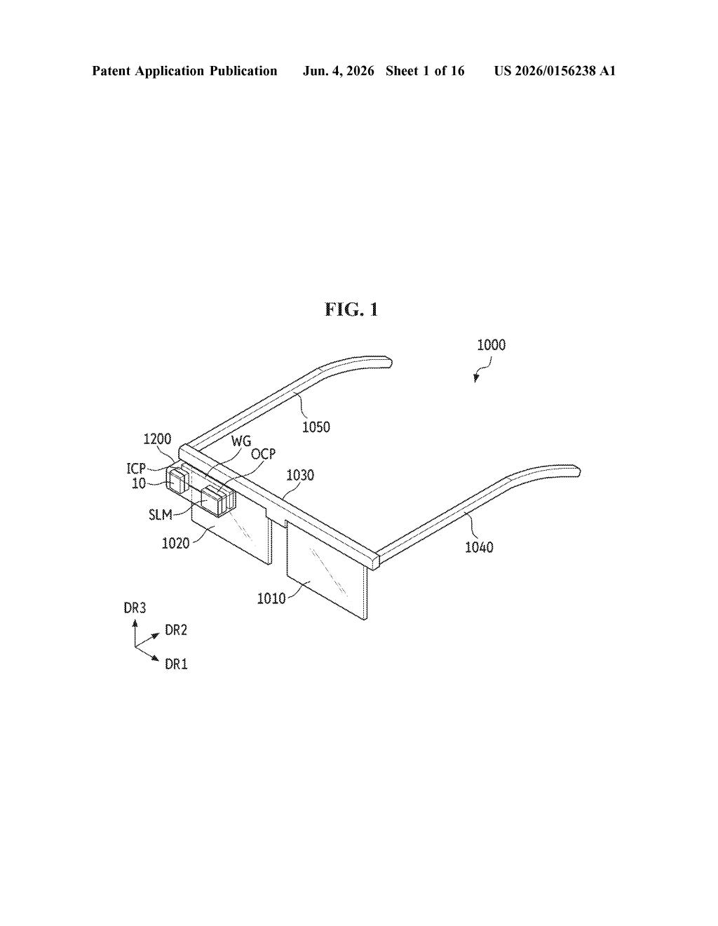
What Samsung's nanostructure waveguide display actually does
Imagine a pair of glasses that project crisp, 3D holographic images into your eyes — but they're slim enough to look like regular frames. The big engineering problem has always been fitting all the optics into something that thin. Bulky lenses and mirrors have to go somewhere.
Samsung's patent describes a system that replaces those bulky components with two sets of nanostructures — microscopic features etched onto surfaces — paired with a thin sheet of glass that bounces light along its length like a fiber optic cable. One set of nanostructures grabs light from a tiny source and aims it into that glass sheet. Another set pulls it back out and aims it precisely at a phase-modulating chip, which is the part that actually sculpts a holographic image.
The result is a compact stack where all the heavy optical lifting happens at the nanoscale, not through centimeters of glass and plastic. That's the key to making a display thin enough to wear comfortably.
How light travels from source to phase modulator
The patent lays out a four-stage optical pipeline inside what would be an extremely thin display panel:
- Light source: A small emitter (likely a laser or LED) provides the raw light.
- First nanostructures: These collimate the light (turn a spreading beam into parallel rays) and redirect its path so it enters a waveguide at the correct angle — think of them as a flat, etched-in replacement for a traditional collimating lens.
- Light guide portion (waveguide): A flat slab that traps light using total internal reflection (the same physics that keeps light inside a fiber optic cable) and carries it from one end to the other.
- Second nanostructures: These extract the light from the waveguide and re-collimate it, directing it precisely at the phase modulator.
- Spatial light modulator (SLM): A chip that controls the phase of incoming light wave-by-wave, which is how holographic displays create the depth and 3D structure of an image.
The Stanford-linked inventors (Gordon Wetzstein runs Stanford's Computational Imaging Lab) bring serious holographic display pedigree to this filing. The architecture is notably close to waveguide-based holographic near-eye display research that's been percolating in academia for several years, now apparently landing in a Samsung Display patent.
What this means for the next wave of AR glasses
AR glasses have been stuck in a size-versus-quality tradeoff for years: either you get decent optics in a bulky headset, or you get slim glasses with a mediocre display. This patent attacks that tradeoff directly. By using nanostructure-based flat optics instead of conventional lenses and by piping light through a thin waveguide, the design keeps the entire optical stack razor-thin — which is the prerequisite for anything you'd actually wear on your face all day.
The inclusion of a spatial light modulator for phase control signals this isn't just a conventional AR overlay system — it's aimed at true holographic display, where images can have real focal depth rather than a flat projection. That matters for eye comfort over long wear sessions, something every AR platform is currently wrestling with.
This is a technically substantive filing, not a broad land-grab. The specific pipeline — nanostructures in, waveguide across, nanostructures out, phase modulator — is a coherent engineering architecture for holographic AR glasses, and the Stanford co-inventors give it real credibility. Samsung Display is clearly thinking beyond flat panels.
Get one Big Tech patent every Sunday
Plain English, intelligent commentary, no hype. Free.
Editorial commentary on a publicly published patent application. Not legal advice.