Nvidia Patents an AI That Reads Chip Wafers for Manufacturing Defects
Every semiconductor wafer that comes out wrong is money lost before a single chip ships. Nvidia's latest patent describes an AI system that watches the manufacturing line and flags defects the moment they appear.
How Nvidia's wafer-inspection AI spots bad chips early
Imagine a factory inspector who never blinks, knows exactly what every part is supposed to look like, and can describe in plain language what went wrong. That's roughly what Nvidia is building for chip manufacturing.
Semiconductor wafers, the silicon discs that get sliced into individual chips, go through dozens of precision steps before they're done. A tiny misalignment, a missing circuit trace, or an overlapping pattern can ruin an entire batch. Today, catching those problems requires specialized equipment and trained human reviewers.
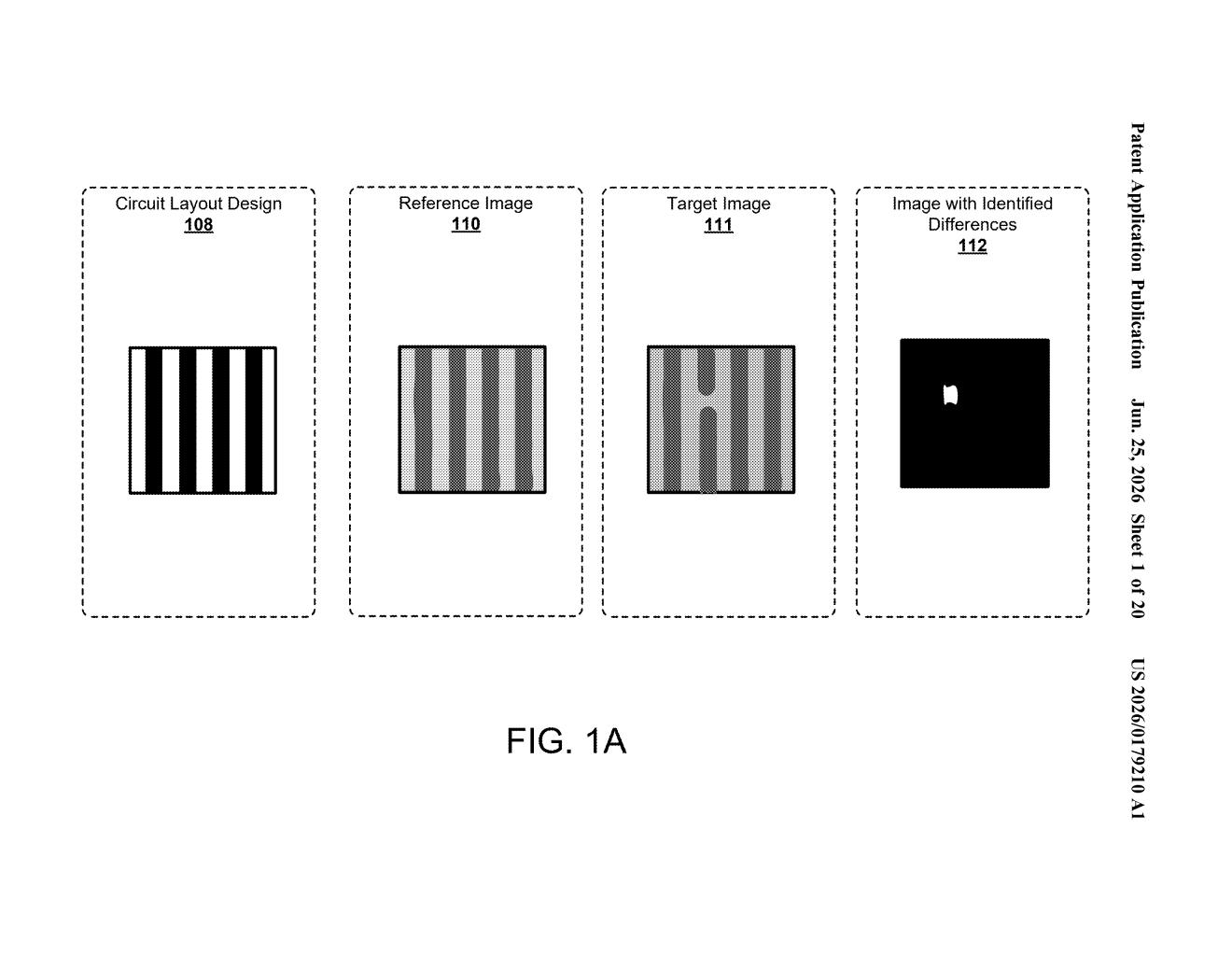
Nvidia's patent describes an AI model that takes in images of a wafer at various stages of production, compares them against what the design should look like, and produces a written description of any problems it finds, including a confidence score. You can even ask it questions in plain text, like prompting it to look for a specific type of defect, and it will focus its analysis accordingly.
How the vision language model flags wafer deviations
The system is built around a vision language model (VLM), a type of AI that can process both images and text at the same time. Think of it like a very focused version of GPT-4o: you show it a photo and ask a question, and it answers based on what it sees.
In this case, the images are microscopy scans of semiconductor substrates (wafers and reticles, the masks used to print circuit patterns). The "question" is a text prompt that tells the model what kind of defect analysis to perform. The model compares the incoming images against reference data, which could be CAD design files, earlier-stage images, or known-good examples, and identifies deviations like:
- Missing circuit features
- Misaligned layers
- Overlapping or smeared patterns
- Unexpected geometric shapes
The patent highlights zero-shot detection (the ability to identify defect types the model was never explicitly trained on) by combining specialized semiconductor datasets with broader general-purpose training data. The system can also monitor a live data stream from manufacturing equipment, not just static images reviewed after the fact.
What this means for chip yield and manufacturing cost
Chip manufacturing yield, the percentage of working chips per wafer, is one of the biggest cost levers in the semiconductor industry. A defect found early in the production process is far cheaper to address than one caught after a wafer has gone through 50 more steps. An AI that can continuously watch the line and describe problems in human-readable terms could dramatically cut the time between a defect appearing and an engineer acting on it.
For Nvidia specifically, this patent sits at the intersection of two things the company is already pushing hard: its AI accelerator business and its emerging physical AI and industrial automation work. A wafer-inspection system built on VLMs could eventually be part of the broader suite of AI tools Nvidia sells to manufacturers, not just something it uses internally.
This is a genuinely practical application of large AI models in a domain where the stakes are high and the existing tools are expensive and slow. The zero-shot capability is the most interesting technical claim: if it holds up, it means the system doesn't need to be retrained every time a new defect pattern shows up on the line. Whether Nvidia pursues this as an internal manufacturing tool or a product to sell to chipmakers is the open question worth watching.
Get one Big Tech patent every Sunday
Plain English, intelligent commentary, no hype. Free.
Editorial commentary on a publicly published patent application. Not legal advice.