
Qualcomm Patents Tiny Built-In Speakers That Push Sound More Precisely
Qualcomm is working on a microscopic speaker component that shapes airflow through its own base, using a stack of precisely sized layers to guide sound more efficiently than a simple drilled hole would.
What Qualcomm's stacked-layer speaker chip actually does
Imagine a tiny speaker built directly into a chip, so small it fits inside a phone or earbud without taking up much space. Getting good sound out of something that size is tricky because the air has to move through a very narrow path, and any turbulence or pressure loss hurts audio quality.
Qualcomm's patent describes a speaker component where the base itself is engineered to fix that problem. Instead of a plain hole punched through the base, the layers are cut at gradually changing sizes, so the opening widens or narrows in steps. That creates a smoother path for air to travel through, which helps the sound come out cleaner.
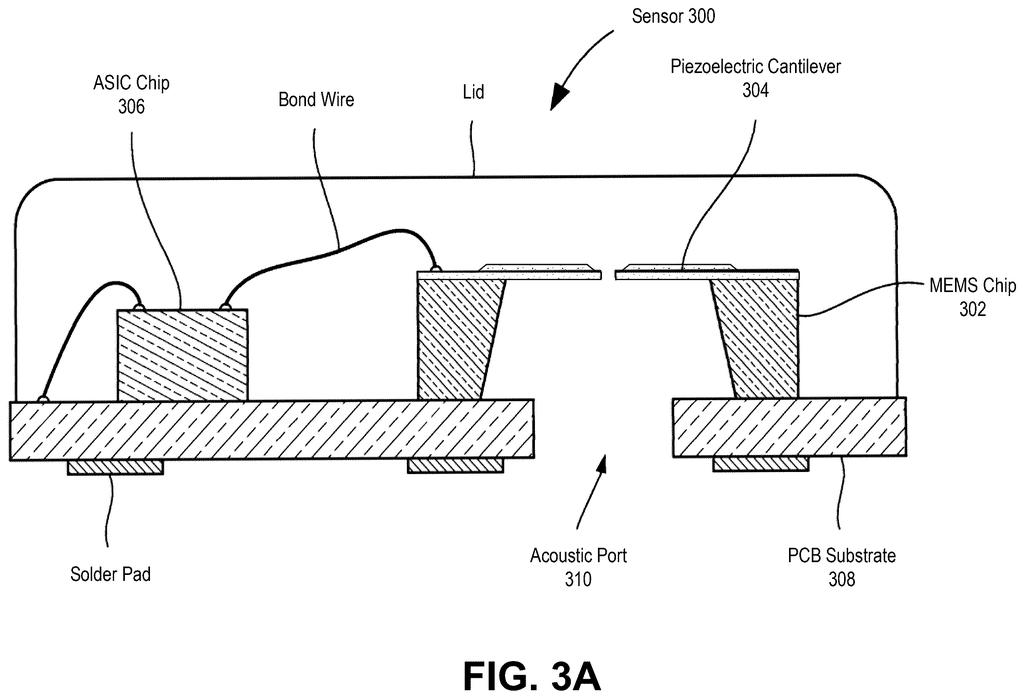
The vibrating part, a thin flexible strip called a cantilever, sits on top and does the actual vibrating. But this patent is mostly about what's underneath, the shaped channel in the base that guides the air it moves.
How the tapered substrate layers shape the sound channel
The patent covers a MEMS transducer (a microscopic device that converts electrical signals into sound) built from two main parts: a transducer body with an internal acoustic cavity running from bottom to top, and a substrate (the layered base the transducer sits on) that includes a precisely shaped hole.
The key invention is in that substrate. Rather than a uniform hole punched straight through, the layers are tapered so each one has a slightly different opening size than the one next to it. This creates a converging or diverging channel, meaning the airflow path either narrows or widens gradually as sound travels through it, instead of hitting a sharp step that causes turbulence or acoustic loss.
The substrate stack includes:
- A solder mask (the outermost protective layer)
- A top metal layer directly beneath it
- Multiple tapered layers below that, each with incrementally different aperture sizes
A piezoelectric cantilever (a thin flexible strip that bends when electricity is applied, generating vibration and therefore sound) sits over the top of the assembly. The combination of a well-shaped air channel in the base and a piezoelectric vibrator on top is what this design is optimizing.
What this means for audio in phones and wearables
MEMS speakers and microphones are increasingly common in earbuds, hearing aids, smartphones, and AR glasses, anywhere engineers want audio in a very small package. The acoustic efficiency of these components directly affects battery life, volume, and sound fidelity. A better-shaped air channel means less energy wasted pushing air through a poorly designed passage, which could translate to a louder or cleaner sound from the same power budget.
For Qualcomm specifically, this kind of work fits its push into audio chips and wearable platforms. If this substrate design improves the acoustic performance of MEMS transducers, it could show up in future Qualcomm reference designs for earbuds or hearing devices, the kind of components that phone and headphone makers build on top of.
This is detailed acoustic engineering work, not a headline product announcement. The tapered-layer approach is a real and specific improvement to a known problem in MEMS audio, but it's the kind of incremental gain that matters most to component engineers rather than end users. Worth watching if you follow the MEMS audio supply chain; easy to skip otherwise.
There are more where this came from
We read every patent application Big Tech publishes and send you the ones worth knowing. Plain English, free, every week.
The drawings
15 drawing sheets from US 2026/0222744 A1 · click any drawing to enlarge


Want this weekly breakdown for a company we don't cover? Patentlyze Pro →