
Samsung Patents a Secure-Write Architecture That Works During Low Power Mode
Most chips stop doing meaningful work when they enter low power mode — but Samsung's new patent describes a way to keep writing security-critical data to non-volatile memory even when the main processor is essentially asleep.
How Samsung keeps security data safe while your device sleeps
Imagine your phone's main brain powering down to save battery, but a small security task still needs to save something important — like a verified record of what software is running on your device. Normally, that kind of write operation needs the full chip awake and involved. This patent describes a way around that.
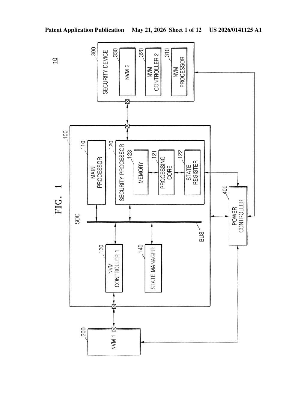
Samsung's design splits the work between a dedicated security device and a lightweight memory processor that can handle secure storage writes on its own, without waking up the main processor. The security data — things like identifiers that confirm which software image is loaded — gets routed through a separate, dedicated channel to its own private memory.
The result is a device that can keep its security bookkeeping up to date even during low power or sleep states, without the energy cost of waking everything up just to write a few bytes of critical data.
How the memory processor handles writes when the SOC is asleep
The patent describes an electronic device architecture with three main components working together: a first NVM (non-volatile memory, meaning storage that survives power loss) that holds both regular program data and a protected security region; a dedicated security device with its own memory, controller, and processor; and a System on Chip (SOC) that houses the main processor, a memory controller, and a separate security processor.
The clever part is what happens in low power mode. Instead of requiring the main processor to stay awake, the security processor inside the SOC sends a write request and the security data directly to the memory processor inside the security device. That memory processor then issues the actual program command, address, and data to the second NVM — all without involving the main CPU.
This creates a clean separation:
- The main processor handles regular app data through one channel
- The security processor offloads sensitive writes through a dedicated security channel
- The memory processor inside the security device executes the write autonomously during low power states
The security region specifically stores identifiers tied to program images — essentially cryptographic receipts that confirm which software was running and when, useful for secure boot and integrity verification.
What this means for secure storage in low-power devices
For devices that need to maintain a tamper-evident log of software state — think embedded systems, secure enclaves in phones, or IoT hardware — the ability to write security data without fully waking the main chip is genuinely useful. It means your device can keep its security records current at lower energy cost, which matters for always-on or battery-constrained hardware.
This architecture also reinforces the trend of isolating security operations from the general-purpose processor entirely. By giving the security device its own memory and processor that can act independently, Samsung reduces the attack surface: even if the main SOC is compromised, the security subsystem keeps functioning on its own terms.
This is solidly useful infrastructure work — not flashy, but the kind of low-level security architecture that matters in embedded and mobile silicon. The specific innovation (autonomous secure writes during low power mode) solves a real constraint in secure boot and integrity logging. It's the sort of thing that quietly ends up in Exynos chips or Samsung's secure element lineup without anyone noticing until a teardown reveals it.
Get our take in your Top Stories
Liked this breakdown? Add Patentlyze as a preferred source on Google, and our plain-English take shows up more often in your Top Stories the next time Samsung patent news breaks.
There are more where this came from
We read every patent application Big Tech publishes and send you the ones worth knowing. Plain English, free, every week.
Want this weekly breakdown for a company we don't cover? Patentlyze Pro →