Sony Patents an Image Processor That Ignores the Parts of a Picture It Doesn’t Need
Most image processors crunch every pixel in a frame, whether it's relevant or not. Sony's new patent describes a chip that skips the parts it's been told to ignore — saving time and power in the process.
What Sony's selective image processing actually does
Imagine a security camera scanning a parking lot. Most of the frame is empty pavement — but the chip still has to process every pixel just to confirm nothing interesting is happening. That's wasted work.
Sony's patent describes an image processor that uses a simple map — a list of flags marking which parts of a picture need processing and which parts can be skipped — to focus its number-crunching only where it counts. You define a target region, and the processor only runs its analysis there.
This kind of selective processing is especially useful in cameras embedded in cars, phones, or surveillance systems, where the processor has to make fast decisions without draining the battery or overheating. By ignoring irrelevant areas, the chip can work faster and more efficiently on the parts that actually matter.
How the flag-data system marks regions to skip
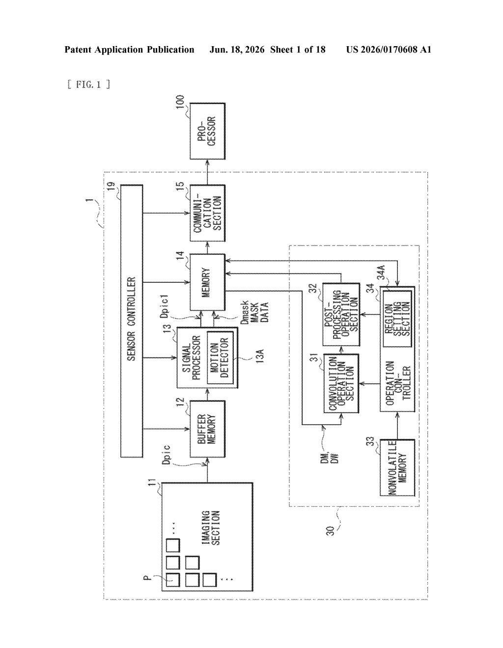
The patent describes two core components working together.
Region setting section: This part reads a piece of "flag data" — essentially a map layered over an image that marks each zone as either "process this" or "skip this." From that map, it defines an operation target region: the specific portion of the image the processor actually needs to work on.
Convolution operation section: Once the target region is defined, this unit runs a convolution operation (the standard math that neural networks use to detect edges, shapes, and objects in images) — but only within the flagged region. It uses the image data alongside a set of weighting coefficients (pre-trained numerical values that tell the system what to look for).
The upshot: instead of running the full computation across an entire image frame, the chip applies it selectively. The flag data acts like a stencil, directing compute resources precisely where they're needed. This architecture fits neatly into embedded vision systems — think automotive cameras, drone sensors, or smartphone camera modules — where processing speed and power draw are tightly constrained.
What this means for camera chips and real-time AI vision
Sony Semiconductor Solutions makes the image sensors inside a huge share of the world's smartphones, cars, and security cameras. A patent like this, focused on reducing wasted computation inside those sensors, is the kind of incremental efficiency work that compounds over time — faster on-device AI, longer battery life, or more accurate real-time detection without needing a more powerful (and expensive) chip.
For you as a consumer, the downstream effect could be a phone camera that processes scenes faster or a car's vision system that reacts more quickly — without the hardware getting bigger or hotter. It's not a flashy idea, but it's exactly the kind of focused optimization that separates good image chips from great ones.
This is unglamorous but genuinely useful chip design work. Sony doesn't file patents for fun — they file them because their sensor business depends on squeezing more performance out of tight power budgets. Selective convolution based on pre-flagged regions is a logical and practical approach, and it's the kind of detail that quietly ends up in the next generation of Sony IMX sensors.
Get one Big Tech patent every Sunday
Plain English, intelligent commentary, no hype. Free.
Editorial commentary on a publicly published patent application. Not legal advice.