
Sony Files Patent for a Camera Chip That Captures and Converts Light in One Step
Sony is filing patents on a way to cram more image-processing circuitry into a camera sensor by splitting the work across two distinct layers of a single chip, a design choice that could shape the sensors inside everything from smartphones to security cameras.
What Sony's two-layer image sensor chip actually does
You're a camera engineer staring at a sensor that needs to do more, faster readout, cleaner signal conversion, less noise, but the chip only has so much surface area to work with. Packing more circuits onto a flat design means something has to give, usually image quality or chip size.
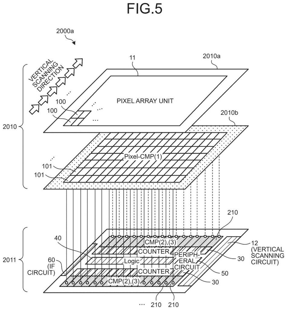
Sony's patent describes a sensor chip that stacks its circuitry vertically rather than spreading it flat. The pixels that actually capture light sit on one layer of the chip. Directly below them, on a second layer of the same physical substrate, are the circuits that read out each pixel's charge and the circuits that begin converting that analog signal into digital data. Everything is organized on a strict one-to-one basis: each individual pixel gets its own dedicated readout circuit.
The result is a more compact sensor that doesn't have to sacrifice processing capability for physical space. You don't see any of this when you hold a phone or camera, but the architecture determines how fast your photos are captured and how clean they look in low light.
photoelectric conversion elements ( 300 ) configured to generate a charge according to received light; a pixel circuit configured to read the charge from the photoelectric conversion element and to convert the charge into an analog type pixel signal …
Translation: The chip captures light with tiny sensors and turns it into a standard electrical wave.
How Sony splits pixel and converter circuits across chip layers
The patent describes an imaging device built on a stacked chip architecture, where different functional layers are physically bonded together as separate tiers within one substrate.
- First layer (top): A matrix array of photoelectric conversion elements, the individual pixels that absorb incoming photons and generate an electrical charge proportional to the light they receive.
- Second layer (bottom, same substrate): Two circuit types live here. The pixel circuit, one per pixel, reads the charge from the photoelectric element above it and converts it into an analog voltage signal. The first circuit (part of the analog-to-digital conversion chain) then processes that analog signal using a reference signal to begin translating it into digital data.
- Second circuit: A downstream stage connected to the first circuit's output that completes the analog-to-digital conversion pipeline.
The key architectural claim is the strict one-to-one correspondence between pixels and their readout circuits, rather than sharing circuits across multiple pixels, each pixel owns its dedicated processing chain. This reduces the cross-pixel interference (called crosstalk) that can blur or corrupt the signal before it ever becomes image data.
The stacking approach is a continuation of a technique Sony has been developing in CMOS image sensors, where separating the light-capturing layer from the processing layer allows each to be optimized independently using different manufacturing processes.
What this means for the next generation of camera sensors
Image sensor architecture is one of those engineering battlegrounds that rarely gets talked about in product announcements but determines almost everything about camera performance. The shift from planar to stacked sensor designs has been one of the most consequential moves in camera chip engineering over the past decade, and Sony has been one of the companies most aggressively pushing it forward. A design that puts dedicated per-pixel processing on a second layer means the sensor can read out pixels faster and with less noise, which translates directly into better video, sharper photos in dark conditions, and reduced motion blur for fast subjects like sports or children.
For Sony Semiconductor Solutions specifically, this matters because the company supplies sensors to a huge portion of the global smartphone and camera industry, including Apple's iPhone lineup. A manufacturing patent that pins down how these layers are arranged and connected is the kind of infrastructure-level filing that protects a process advantage for years. Imaging sensor filings like this one are part of the ongoing wave of new Big Tech patents reshaping how camera hardware is designed at the chip level.
Flat sensor designs force trade-offs between pixel density, readout speed, and signal quality that engineers have been fighting for years, so the problem here is measurable and well known. Stacking layers is a known solution, but the specific arrangement, placing both the pixel readout circuit and the first stage of analog-to-digital conversion together on the second layer, tied one-to-one with each pixel, is a serious architectural commitment. Whether this configuration represents a manufacturing leap or an incremental refinement depends heavily on what Sony can actually achieve in fabrication, which a patent alone can't confirm.
There are more where this came from
We read every patent application Big Tech publishes and send you the ones worth knowing. Plain English, free, every week.
The drawings
40 drawing sheets from US 2026/0238902 A1 · click any drawing to enlarge


Want this weekly breakdown for a company we don't cover? Patentlyze Pro →
Be the first to weigh in