Samsung Patents an AI System That Finds Hidden Defects Using Ultrasound
Samsung has filed a patent for a defect detection system that bounces ultrasonic waves through a material, processes the echoes with AI, and flags hidden flaws — all without cutting the part open.
What Samsung's ultrasonic defect scanner actually does
Imagine you need to check whether a metal component — say, a chip package or a structural part — has tiny cracks or voids hiding inside it. You can't see them with your eyes, and cutting it open to look defeats the purpose.
This is what ultrasound inspection is for. Samsung's patented system fires ultrasonic pulses at the material, listens for how the sound bounces back, and then feeds those echo signals into an AI model trained to recognize the difference between a healthy return signal and one that hints at a defect buried inside.
The clever part is how it prepares the data before the AI ever sees it. The system trims, labels, scales, and merges the raw echo signals into a clean dataset, then uses a statistical technique called principal component analysis to pinpoint where defects are likely hiding. That labeled dataset trains the deep learning model, so the whole process — from raw sound data to defect location — becomes largely automatic.
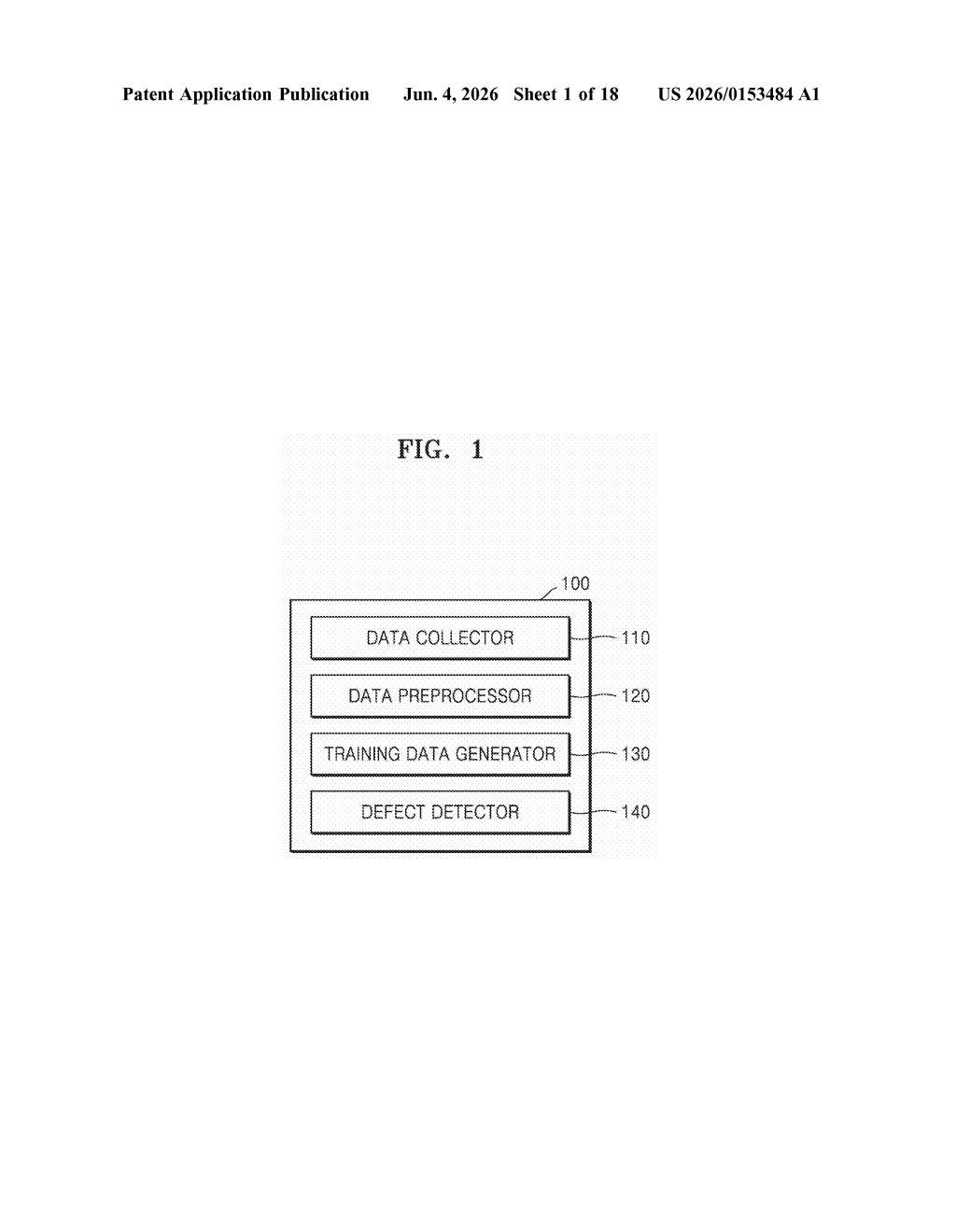
How the system turns sound echoes into a defect map
The system works in four sequential stages, all handled by a single processing unit:
- Data collection: An amplitude-mode (A-mode) ultrasonic transducer scans across the test subject, recording reflected signal data at each position. A-mode ultrasound gives you a simple amplitude-vs-time waveform — think of it like a sonar ping that shows how far away a reflective surface is and how strongly it bounced back.
- Preprocessing: The raw signals are trimmed to relevant windows, assigned positional identifiers, amplitude-normalized (so signals from different scan positions are on a consistent scale), and merged into a unified dataset.
- Training data generation: Principal component analysis (PCA) — a dimensionality-reduction technique that finds the most statistically significant patterns in a dataset — is run on the merged signals to locate where defects sit within the material. The system then labels each merged signal as either defect-including or defect-free, producing a labeled training dataset.
- Deep learning inference: A deep learning model is trained on that labeled dataset and then used to detect defects in new test subjects.
The self-contained pipeline is notable because the system generates its own training labels from PCA analysis rather than requiring manual human annotation — a common bottleneck in industrial inspection workflows.
What this means for automated manufacturing inspection
Industrial defect inspection is one of those unglamorous problems that costs manufacturers a lot of money. Manual ultrasonic inspection requires trained technicians, is slow, and is hard to scale. Systems that automate the full pipeline — from raw signal to defect label to trained model — directly reduce that cost and can be integrated into high-throughput production lines.
For Samsung specifically, this kind of technology is relevant to semiconductor packaging and component quality control, where hidden delaminations or voids inside chip packages can cause field failures. A self-training inspection module that doesn't require a pile of pre-labeled data to get started is a meaningful step toward fully automated quality gates on a fab floor.
This is solid, practical engineering work aimed squarely at reducing the human labor required to set up automated inspection systems. The self-labeling via PCA is the genuinely interesting bit — it sidesteps the tedious manual annotation problem. It won't make headlines, but it's exactly the kind of IP that quietly ends up embedded in production line equipment.
Get one Big Tech patent every Sunday
Plain English, intelligent commentary, no hype. Free.
Editorial commentary on a publicly published patent application. Not legal advice.