Samsung's Latest Patent Pulls the Control Chip Off the Screen Itself
Samsung Display has filed a patent that physically separates the chip controlling a screen from the screen itself — both sitting on a shared transparent base. It's a subtle architectural shift that could matter a lot for future foldable, transparent, or ultra-thin displays.
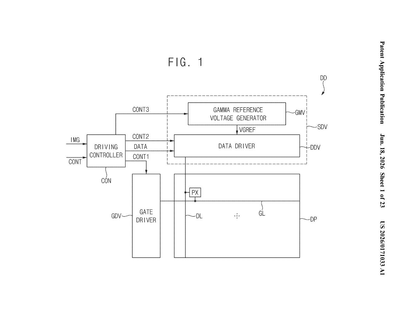
What Samsung's off-panel display driver actually does
Think about the screen on your phone. The tiny chip that tells each pixel when to light up is normally attached right at the edge of the screen panel — almost glued to it. Samsung's patent describes pulling that chip away from the panel and placing it separately on the same clear backing material, then running wires across that backing to connect the two.
The key word is transparent substrate — a clear, flat base layer that holds both the screen panel and its driver chip at the same time. Because the base is see-through, it doesn't visually block anything even if it extends beyond the visible screen area.
This kind of layout gives engineers more flexibility in how they shape, fold, or layer a display. Instead of everything being crammed into one tight assembly, the driver chip can live in a less visible or less mechanically stressed spot — potentially making screens thinner, more foldable, or even partially see-through.
How the transparent substrate ties the driver to the panel
The patent describes a display device built around three main components, all sharing a single transparent substrate:
- Display panel — the visible part of the screen, divided into a lit-up display area (where pixels live), a surrounding non-display border zone, and a pad area where electrical contacts are made.
- Driving controller — the chip that sends signals telling each pixel what color and brightness to show. Crucially, it sits apart from the display panel on the same transparent base, rather than being bonded directly to the panel's edge.
- Connecting lines — thin conductive traces running across the transparent substrate from the driving controller to the pad area of the display panel, carrying the signals between the two.
The distinction from conventional designs is physical separation. In most displays today, the driver IC (integrated circuit) is bonded directly to the panel's edge in a process called chip-on-glass or chip-on-film. Here, both the panel and the driver share a transparent floor but are discrete, spaced-apart units bridged by printed wires.
The transparent substrate is central to why this works aesthetically and optically — it doesn't add an opaque layer that would obscure any see-through design intent.
What this means for thinner or see-through screens
Separating the driver from the display panel is the kind of structural decision that quietly enables a new class of form factors. Transparent displays — used in retail windows, automotive heads-up displays, and experimental AR screens — need every layer to carry as little visual obstruction as possible. Putting the driver chip on the same clear base without bonding it to the panel edge keeps that transparency intact while still maintaining a compact assembly.
For foldable or rollable screens, moving the driver away from the most mechanically stressed fold zone could also improve durability. A chip bonded at a fold point is a reliability risk; one sitting on a stiffer, separate section of the same substrate is not. Whether this shows up in a phone, a wearable, or a commercial display panel first is unclear from the patent alone — but the geometry it describes fits squarely with where display engineering is heading.
This is foundational display-architecture work — not flashy, but the kind of structural patent that precedes real product changes. Samsung Display supplies screens to Apple, Google, and its own Galaxy line, so a new substrate layout approach here has a wide potential blast radius. That said, the claim as written is fairly broad and describes a configuration rather than a novel process, which may make it harder to defend if challenged.
Get one Big Tech patent every Sunday
Plain English, intelligent commentary, no hype. Free.
Editorial commentary on a publicly published patent application. Not legal advice.