Sony Patents a Laser Chip Design That Keeps Its Base from Warping
When you stack thin semiconductor layers on a chip, they can pull or push the base like a bimetallic strip — bowing it out of flat. Sony's new patent tackles that exact problem for a class of lasers used in depth sensors and optical communications.
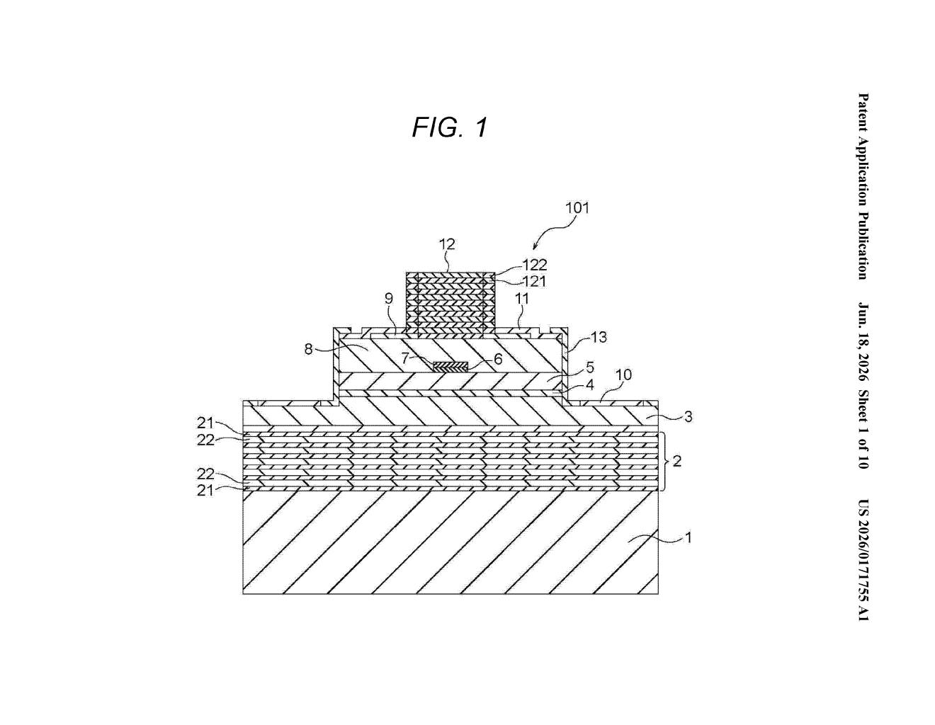
What Sony's anti-warp laser structure actually does
Imagine stacking thin sheets of different materials on top of each other. Each sheet expands or contracts at a slightly different rate, and over time the whole stack bends like a wet piece of cardboard. That's a real problem when you're building tiny lasers called VCSELs — the kind used in Face ID-style depth sensors and fiber-optic links — because a warped base means fewer working chips per wafer, and chips that do work may not perform consistently.
Sony's patent describes a way to engineer the bottom layers of the laser stack so the bending forces cancel each other out. One layer is chosen because its crystal structure is slightly too big for the base; another is chosen because it's slightly too small. Together they hold each other in tension and keep the whole base flat.
The result, according to Sony, is a flatter wafer, more consistent performance across the entire surface, and better manufacturing yield — meaning more good chips come out of each production run.
How opposing crystal layers cancel out substrate stress
A VCSEL (Vertical-Cavity Surface-Emitting Laser) is a laser that shoots light straight up through the surface of a chip rather than out the side. VCSELs are used in depth-sensing cameras, LiDAR, and high-speed data links. They're built by depositing dozens of ultra-thin semiconductor layers on a GaAs (gallium arsenide) substrate — a crystalline wafer that acts as the foundation.
The problem Sony is solving is substrate warpage. Different semiconductor materials have different lattice constants (the natural spacing between atoms in the crystal). When you grow a layer whose atoms are spaced slightly differently from the substrate beneath it, mechanical stress builds up — and enough stress bends the whole wafer. A bent wafer is harder to process and produces chips with uneven characteristics.
Sony's fix lives in what the patent calls the first semiconductor stacked structure — a buffer zone between the GaAs base and the active laser layers above. This buffer intentionally includes:
- A 1-1st layer with a lattice constant larger than GaAs (pushing outward)
- A 1-2nd layer with a lattice constant smaller than GaAs (pulling inward)
The opposing stresses offset each other, keeping the wafer flat. Above this compensated buffer sits the active laser region, which contains InP (indium phosphide) — a material well-suited to infrared wavelengths but normally tricky to combine with GaAs without introducing warp.
What this means for laser sensors in Sony products
VCSELs are already inside millions of consumer devices — Apple uses them for Face ID, Sony uses them in PlayStation camera accessories and sensors — and demand is growing for longer-wavelength versions that work in optical data centers and automotive LiDAR. The catch is that longer-wavelength VCSELs typically need materials like InP that don't naturally sit flat on a GaAs base. Sony's stress-balancing approach could make those mixed-material designs manufacturable at scale.
For you as a consumer, better yield and more uniform chips mean the sensors in future devices are more likely to work reliably at a lower cost. This is the kind of quiet manufacturing patent that rarely makes headlines but directly influences whether a technology stays expensive or becomes mainstream.
This is a solid, specific manufacturing patent — not flashy, but exactly the kind of foundational work that determines whether a technology scales. Sony has genuine expertise in laser manufacturing, and a patented approach to stress compensation in mixed-material VCSELs is a real competitive asset as the industry pushes toward longer-wavelength sensors.
Get one Big Tech patent every Sunday
Plain English, intelligent commentary, no hype. Free.
Editorial commentary on a publicly published patent application. Not legal advice.