Sony's New Patent Packs a Full Depth-Sensing Camera onto a Single Chip
Sony is working on a way to pack an entire light-based depth sensor — the kind used in self-driving cars and face-ID cameras — onto a single silicon chip, with a built-in shield to stop stray light from corrupting the measurement.
What Sony's all-in-one light-based distance sensor does
Imagine a bat using sonar: it sends out a sound pulse, waits for the echo, and calculates how far away an object is from how long the echo took to return. LiDAR works the same way, but with pulses of light instead of sound. It's what lets your iPhone scan your face in 3D, and what helps self-driving cars "see" the road.
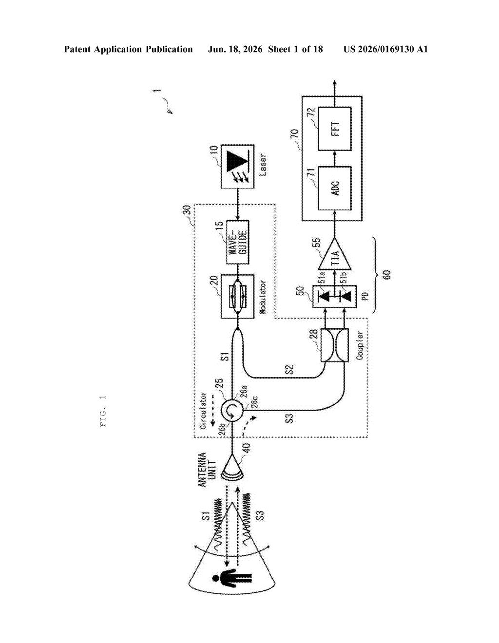
Right now, LiDAR systems typically need several separate parts — a laser, a detector, and the plumbing to connect them — spread across multiple components. Sony's patent describes squeezing all of that onto one silicon chip: a light guide (called a waveguide) carries the laser pulse to a tiny antenna that fires it outward, and a separate receiver on the same chip catches the returning reflection.
The clever addition is a light-blocking section built around the antenna and receiver. Without it, the outgoing light pulse could bounce around inside the chip and muddy the incoming signal — like trying to hear a faint echo while someone is still shouting. The shield keeps the two signals cleanly separated.
How the chip sends, bounces, and catches light to measure depth
The patent describes a photodetector — essentially a depth-sensing chip — built entirely within a silicon substrate. That single chip contains three key pieces working together:
- Optical waveguide: A microscopic channel etched into the silicon that carries laser light from a source to the right spot on the chip, the way a fiber-optic cable carries light over long distances.
- Optical antenna: A structure that takes the guided light and fires it outward as a beam toward whatever object the sensor is pointed at.
- Light-receiving element: A photodetector that picks up the portion of the beam that bounces back from the object. By measuring the round-trip time of that pulse, the chip can calculate distance.
The fourth ingredient — the light-blocking section — sits around the antenna, the receiver, or both. Its job is optical isolation: preventing the outgoing laser signal from leaking sideways across the chip and reaching the receiver before the real reflected signal does. That kind of crosstalk (unwanted internal interference) would make distance readings inaccurate or noisy.
All of this sits in a silicon substrate, which matters because silicon-based manufacturing is the same process used to make standard camera image sensors — meaning this design could, in principle, be produced at scale using existing fabrication lines.
What this means for cameras, robots, and AR devices
Distance sensors are showing up in more consumer devices every year — from the Face ID dot projector on iPhones to the depth cameras on AR headsets and the obstacle-avoidance systems in robots and drones. Making them smaller and cheaper is the main barrier to putting them everywhere.
A fully integrated, single-chip design like this one could reduce the size and assembly cost of LiDAR modules significantly. For Sony specifically — a company that already supplies image sensors to Apple, Samsung, and others — this kind of chip could slot into a future camera module or sensor array. The light-blocking innovation is the practical detail that makes a compact design actually work, because shrinking everything down is only useful if the signals don't interfere with each other.
This is solid, focused engineering work rather than a headline-grabbing concept. Sony is one of the world's dominant image-sensor suppliers, so a patent that extends their silicon expertise into depth sensing is a natural and credible move. The light-blocking detail is the part worth paying attention to — it's the kind of unglamorous problem that actually determines whether a compact sensor is usable in the real world.
Get one Big Tech patent every Sunday
Plain English, intelligent commentary, no hype. Free.
Editorial commentary on a publicly published patent application. Not legal advice.