Sony Patents a Camera Chip That Combines Two Light Captures Before Saving a Photo
Sony's latest patent describes an image sensor that quietly blends two separate pixel readings together inside the chip itself — before the data ever reaches the processor. It's a small architectural choice with potentially meaningful consequences for image quality.
What Sony's dual pixel signal merger actually does
Imagine your camera taking two quick readings of the same scene and then averaging them together to reduce noise. That's roughly the idea here, but Sony's patent describes doing that combining step inside the sensor chip itself, rather than handing two separate readings off to a processor to merge later.
The chip uses two dedicated memory circuits — called sample and hold circuits — to temporarily store each of the two pixel readings. A control circuit then combines them into a single, blended signal. Think of it like a barista pulling two espresso shots and combining them in the cup before handing it to you, rather than handing you two separate cups to mix yourself.
Doing the merge on-chip can mean less data needs to travel to the main processor, which is faster and can reduce the kinds of errors that creep in during data transfer. Whether this ends up in a Sony camera, phone sensor, or something else entirely isn't specified in the patent.
How the sample-and-hold circuits capture and combine signals
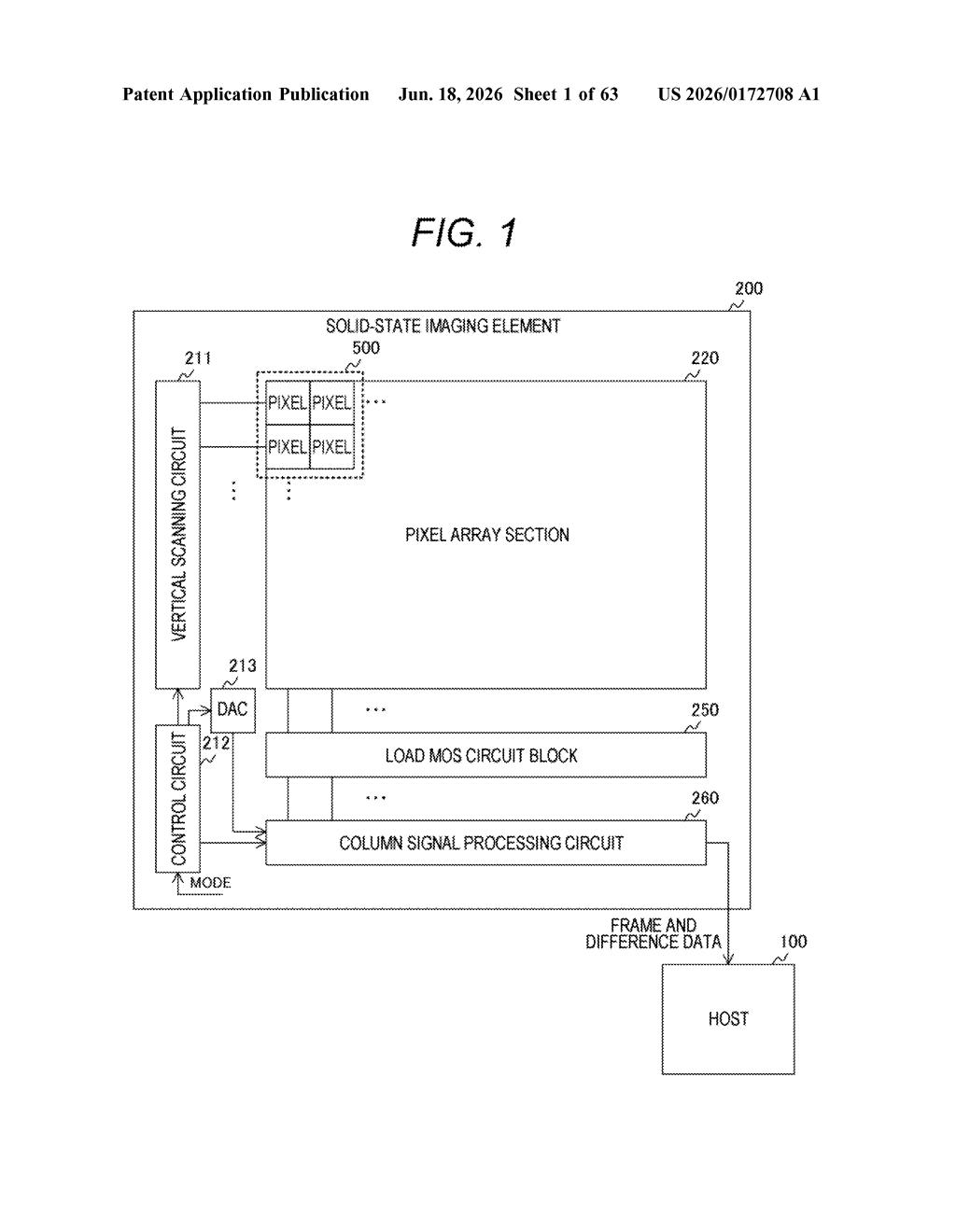
The patent describes a solid-state imaging element — the kind of chip found inside digital cameras and smartphones — with a specific architectural addition: two independent sample and hold circuits.
A sample and hold circuit is essentially a tiny, fast memory cell. When a pixel generates a voltage signal (its reading of how much light hit it), the sample and hold circuit grabs that value and holds it steady long enough to be processed. This patent adds a second such circuit so that two separate pixel signals can be captured and held simultaneously.
The key component is a vertical scanning circuit — a controller that coordinates which rows of pixels are read and when. In this design, that scanning circuit also orchestrates the two sample and hold circuits to produce a combined signal: a single output derived from both pixel readings.
The patent doesn't specify exactly how the signals are combined (averaged, summed, or otherwise), but the core claim is that this combination happens within the imaging element itself, before the signal leaves the sensor. This on-chip approach is distinct from software-based multi-frame merging done after the fact.
What this means for camera sensor performance
On-chip signal combining can reduce the amount of raw data that needs to be shuttled off the sensor to a separate processor, which in practice can mean faster readout speeds and less opportunity for noise to corrupt the data in transit. For applications like high-speed video, scientific imaging, or low-light photography, shaving off processing steps early in the pipeline has real value.
That said, this is a foundational circuit-architecture patent — it describes a structure, not a finished product. Sony Semiconductor Solutions supplies image sensors to a wide range of device makers, so if this design makes it into production, you might encounter it inside a smartphone, a security camera, or a medical imaging device without ever seeing Sony's name on the box.
This is a low-level hardware patent covering a specific circuit arrangement inside an image sensor. It's not flashy, and Sony files many patents like this every year. The concept of combining pixel signals to reduce noise is well-established; what this patent claims is a particular on-chip implementation using dual sample-and-hold circuits under a scanning controller. Worth a note if you follow image sensor architecture, but don't expect a headline product announcement tied to it.
Get one Big Tech patent every Sunday
Plain English, intelligent commentary, no hype. Free.
Editorial commentary on a publicly published patent application. Not legal advice.