Samsung Patents an AI Training Method That Matches Defect Patterns on Chip Wafers
When a batch of chips comes out of a factory with defects, engineers spend hours hunting through thousands of previous wafer maps to find similar failures. Samsung is training an AI to do that search automatically.
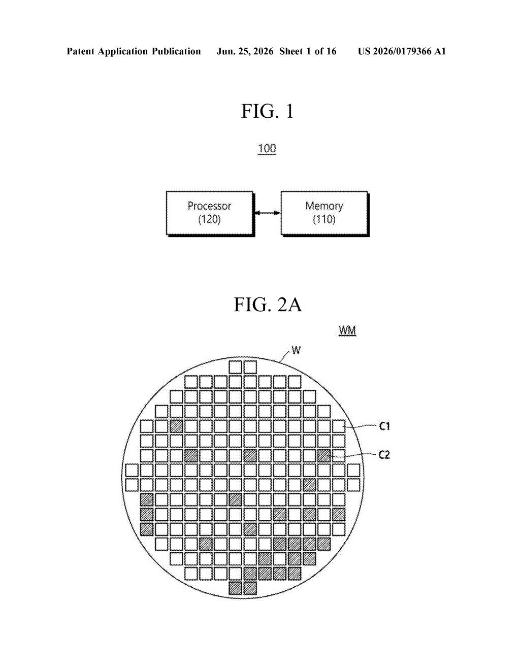
What Samsung's wafer defect-matching AI actually does
Imagine a semiconductor factory where circular silicon wafers come off the production line with tiny defects scattered across them. Engineers map those defects visually, and when something goes wrong, they need to find older wafers with the same defect pattern to understand the root cause. That search, done manually, is slow and inconsistent.
Samsung's patent describes a way to train an AI model to recognize which wafer defect maps look like each other. The trick is a pre-training step: the system blurs all the maps first, then sorts them into "matches" and "non-matches" based on how similar their pixel patterns are. The AI learns from those sorted pairs before it ever sees a real, unblurred wafer.
The blurring step is doing something clever: it strips away fine noise and lets the model focus on the overall shape of a defect pattern rather than tiny pixel-level accidents. That means the AI builds a more reliable intuition for what "similar" actually looks like across thousands of wafers.
How blurring wafer maps trains the similarity model
The patent describes a two-stage training pipeline for a deep learning model used in semiconductor quality control.
Stage one (pre-training): The system takes a large library of wafer maps (visual diagrams showing where defects landed on a silicon disc) and blurs all of them. It then picks a target map and automatically labels every other blurred map as either a positive match (high pixel similarity to the target) or a negative match (low similarity), using a pixel-based similarity index (a numerical score comparing how closely two images overlap). The model trains on these labeled pairs.
Why blur first? Raw wafer maps contain small, random pixel noise that can confuse a similarity model. Blurring acts as a filter, making the broad defect pattern (a ring of failures, a cluster in one corner) stand out over random speckle. The model learns the signal, not the noise.
The downstream goal is a model that, given a new defective wafer, can quickly surface the most similar historical wafers from a database. Engineers use those matches to trace recurring manufacturing problems back to specific tools, chemicals, or process steps.
What this means for semiconductor yield and quality control
Semiconductor yield (the percentage of chips that pass inspection) is one of the most important cost levers in the industry. Identifying recurring defect patterns faster means engineers can catch a manufacturing problem before it ruins an entire production run, not after. A reliable AI search tool compresses that diagnosis from hours to seconds.
For Samsung, which runs some of the world's largest chip fabrication facilities, this kind of internal tooling has direct financial consequences. The patent is narrow in scope (a training method, not the model itself), but it reveals that Samsung is investing in automated defect analysis at the AI infrastructure level, which points toward more autonomous quality control systems in its fabs.
This is a focused, unglamorous engineering patent aimed squarely at Samsung's chip manufacturing operations. It won't show up in a consumer product, but the problem it solves (finding matching defect patterns across huge wafer libraries) is real and expensive. The blurring-as-pre-training trick is a sensible solution worth noting, even if it won't win any AI research prizes.
Get one Big Tech patent every Sunday
Plain English, intelligent commentary, no hype. Free.
Editorial commentary on a publicly published patent application. Not legal advice.