Samsung Patents an AI Training Method for Matching Chip Defect Patterns
Every silicon chip starts life on a wafer, and every defective chip leaves a telltale pattern. Samsung is patenting a smarter way to teach an AI to recognize when two defect patterns are the same kind of problem.
What Samsung's wafer defect-matching AI actually does
Imagine a hospital pathologist who has seen thousands of X-rays. Over time, they get very good at spotting when two scans show the same kind of problem, even if the images look slightly different. Samsung is trying to build the AI equivalent of that pathologist, but for semiconductor wafers.
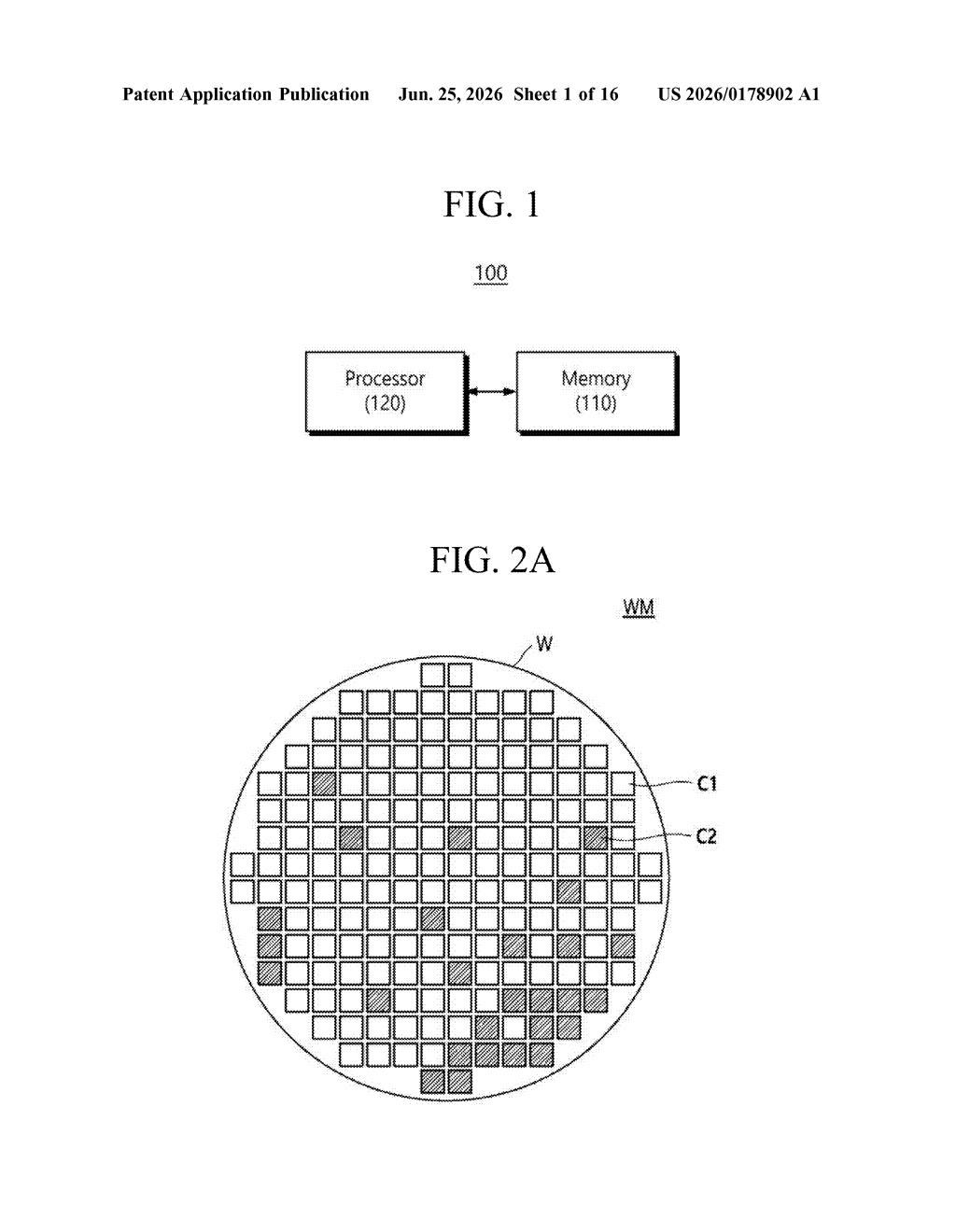
A wafer map is essentially a picture of a circular silicon disc showing where defects landed during manufacturing. When many chips on the same wafer fail in the same spatial pattern, it usually points to a specific equipment or process problem. Finding similar patterns across batches helps engineers diagnose what went wrong.
This patent describes a training technique where the AI is shown wafer maps that have been intentionally blurred before it learns from them. By learning from softened images first, the model builds up a general sense of defect shapes before getting exposed to sharp, noisy real-world data. Think of it as making a student study simplified diagrams before handing them the messy real thing.
How blurring wafer maps trains the similarity model
The patent describes a two-stage training approach for a deep learning model designed to judge whether two wafer defect maps look alike.
Stage one (pre-training): The system takes a large set of wafer maps and blurs them all. It then uses a pixel-based similarity index (a straightforward mathematical measure of how closely two images match pixel by pixel) to sort them into pairs. Maps that score high similarity to a chosen "target" map become the positive set (these should match). Maps that score low become the negative set (these should not match). The model is trained on these labeled pairs.
Why blur first? Raw wafer maps are noisy and high-detail. A pixel-level comparison on raw images can be fooled by tiny irrelevant differences. Blurring smooths out that noise, making the pixel similarity score a more reliable training signal for capturing the broader defect shape.
- Blurred maps reduce noise that would mislead the similarity score
- Positive and negative sets give the model clear examples of "same pattern" vs. "different pattern"
- Pre-training on blurred data builds a generalizable foundation before fine-tuning on real images
The result is a model that can take a new wafer map and retrieve the most similar historical maps from a database, helping engineers trace recurring defect types to their root causes.
What this means for semiconductor yield and quality control
Semiconductor manufacturing runs on yield: the percentage of chips on a wafer that actually work. When a new defect pattern appears on the production line, engineers need to figure out fast whether they've seen it before and what caused it. Today that matching is often done manually or with simpler rule-based tools. An AI that can reliably retrieve similar historical maps could shorten that diagnosis cycle from days to hours.
For Samsung specifically, this kind of internal tooling matters at the scale it operates. The company fabricates chips for its own products and as a contract manufacturer for others. Better defect-pattern matching means fewer bad wafers making it downstream, which translates directly to cost savings and faster process improvement across its fabs.
This is solidly useful internal manufacturing tooling, not a consumer-facing technology story. The blurring-before-training insight is a neat practical trick for improving training data quality, but it's incremental rather than a directional bet. If you follow semiconductor process engineering or AI applications in manufacturing, it's worth a look. General-interest readers can safely move on.
Get one Big Tech patent every Sunday
Plain English, intelligent commentary, no hype. Free.
Editorial commentary on a publicly published patent application. Not legal advice.