Sony Files Patent for an Image Sensor That Converts Light to Data Faster
Every photo your camera takes involves a race to convert raw electrical signals into digital numbers before the next frame arrives. Sony's new patent describes a way to run that race faster without the image-quality tradeoffs that usually come with speed.
What Sony's variable-attenuation image sensor actually does
Imagine a camera sensor as a giant grid of tiny buckets, each collecting light. Once the shutter fires, every bucket has to report its contents as a number before the camera is ready for the next shot. The circuit that does that reporting is called an analog-to-digital converter, and making it fast without making it noisy is one of image-sensor engineering's classic headaches.
Sony's patent describes a redesigned version of that conversion circuit. Instead of treating every signal the same way, it adjusts how aggressively it scales the signal down based on how bright or dim that part of the scene is. A second circuit mirrors that scaling on the reference side, and a comparator figures out where the two meet. The result is a digital reading that arrives quicker and more accurately across a wider range of light levels.
This kind of improvement tends to matter most in fast-moving situations, like sports, video, or anything shot in tricky lighting. Better analog-to-digital conversion at the sensor level means less noise and more detail before any software processing even begins.
How the two attenuation circuits speed up conversion
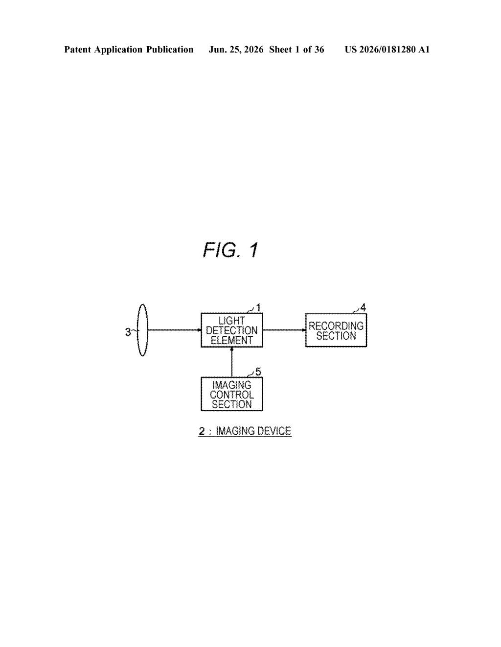
The patent centers on a light detection element (essentially one pixel's readout circuit) that contains four main parts working together.
- First attenuation circuit: Takes the raw electrical signal from the photodetector and scales it down by one of several possible rates, chosen automatically based on how strong the signal is. Think of it as a volume knob that adjusts itself depending on whether the sound is a whisper or a shout.
- Second attenuation circuit: Does the same thing to a stable reference signal, but its scaling rate is controlled by a separate control signal rather than the input itself. This gives the circuit a moving target to compare against.
- Comparator: Watches both scaled signals and notes when they cross each other. That crossing point encodes the brightness of the pixel.
- Counter: Turns the comparator's timing data into a final digital number representing that pixel's light level.
The key innovation is the variable attenuation on the input side. Traditional single-slope analog-to-digital converters (which count up a ramp signal until it matches the pixel voltage) use a fixed reference ramp, which takes longer for brighter pixels. By scaling the input signal adaptively, Sony's design can compress the conversion time while keeping accuracy intact.
What this means for cameras and image sensors
Faster analog-to-digital conversion at the pixel level means a camera sensor can read out a full frame more quickly, which directly affects how fast a camera can shoot continuous frames, how cleanly it can record high-frame-rate video, and how well it handles rolling shutter distortion (the bending effect you see when panning quickly). These are real pain points in everything from smartphone cameras to professional cinema sensors.
Sony Semiconductor Solutions is one of the world's largest image sensor suppliers, making the chips inside cameras from Apple, Google, and many others. A core readout-circuit improvement like this, if it reaches production, would filter into a wide range of devices rather than one specific product line.
This is a genuine low-level engineering patent, not a flashy feature announcement, but low-level engineering is where Sony's real competitive advantage lives. Improving analog-to-digital conversion efficiency is the kind of incremental gain that compounds across an entire sensor product line, and Sony is the company whose sensors end up in the most-used cameras on the planet.
Get one Big Tech patent every Sunday
Plain English, intelligent commentary, no hype. Free.
Editorial commentary on a publicly published patent application. Not legal advice.