
Samsung Display Patents a Pixel Design That Separates Brightness from Light Output
Samsung Display has patented a pixel circuit design that adds a dedicated transistor to control exactly when each pixel connects its brightness-setting stage to its light-emitting stage. It's a subtle architectural change, but in the world of OLED displays, that kind of precision matters.
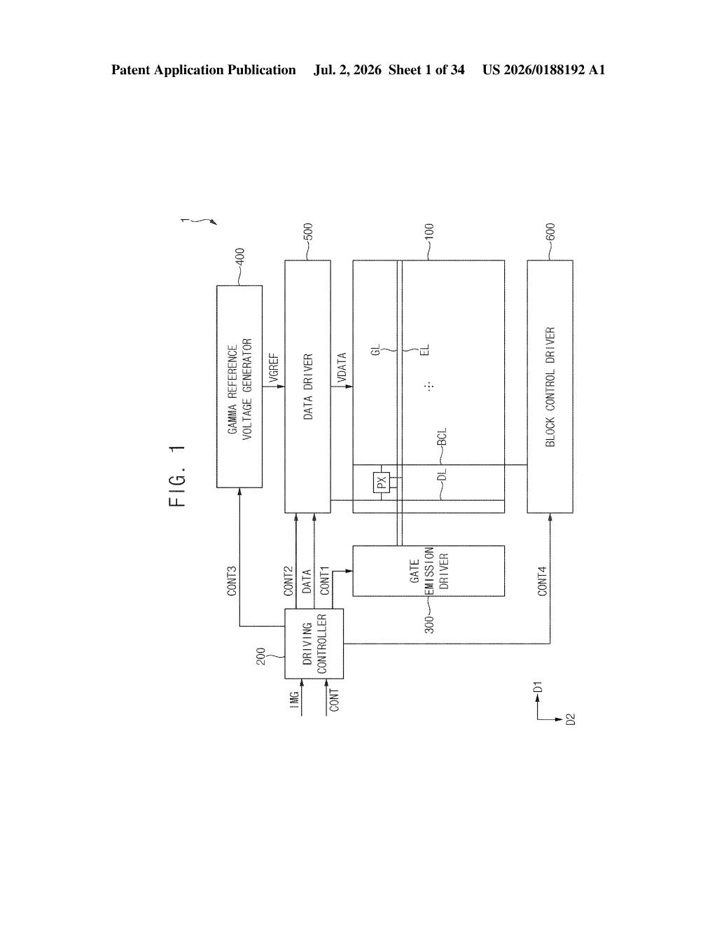
What Samsung's block control pixel circuit actually does
Imagine a dimmer switch in your home where the dial that sets the brightness is on a completely separate circuit from the bulb itself. Right now they're wired together, which means any noise or timing glitch in one can mess up the other. Samsung's patent describes a display pixel that works more like that separated setup.
Each pixel on a screen is its own tiny circuit that does two jobs: figure out how bright to be (set by incoming data), and actually glow at that brightness. Samsung's design adds a dedicated "block control" transistor that acts like a gate between those two jobs, connecting them only at exactly the right moment.
The result is more precise control over when a pixel charges up versus when it emits light. That kind of timing control is a common engineering target in high-end OLED panels, where uneven charging or timing bleed between pixels shows up as flickering, uneven brightness, or ghosting.
How the four-transistor pixel circuit controls light output
The patent describes a display panel where each pixel circuit contains four key transistors working in a specific sequence.
- Driving transistor: controls how much current flows to the light-emitting element (an OLED) based on the voltage stored at a node called the "first node."
- Block control transistor: the new addition. It connects the first node to a second node only when a dedicated block control signal is active, keeping the charging stage isolated from the brightness-control stage until the timing is right.
- Write transistor: loads the brightness data (the data voltage) onto the second node when a write gate signal fires.
- Reset transistor: clears the second node by applying a reference voltage before each new frame, wiping the slate clean.
A dedicated block control driver sits at the panel level and coordinates when the block control transistor opens or closes across all pixels. The driving controller ties together this driver, the data driver, and the gate emission driver based on timing signals from the main processor.
The separation of the write and block control signals means the pixel can be written with new data while the previous brightness setting is still being held stably, reducing interference between the two operations.
What this means for OLED display quality and power use
In OLED displays, the biggest enemies of image quality are timing leakage and charge instability inside the pixel circuit. When the transistors that handle incoming brightness data are too closely coupled to the transistors that control light output, noise from one stage bleeds into the other. That's what causes subtle flickering, color shifts at low brightness, and the kind of image artifacts that show up in high-refresh-rate or variable-refresh-rate modes.
Samsung Display is the world's largest OLED panel supplier, shipping screens into Samsung Galaxy phones, tablets, and products from Apple and other OEMs. A pixel circuit architecture patent like this tends to work its way into production panels over a product cycle or two. If the block control approach meaningfully reduces charge interference, you'd expect to see the benefit in low-brightness accuracy and high-refresh stability on future panels.
This is a fairly deep-in-the-stack display engineering patent, not a user-facing feature you'd ever see named on a spec sheet. But Samsung Display's pixel circuit architecture directly determines the image quality ceiling for every device that uses its panels, which is a lot of devices. It's worth tracking for anyone who follows OLED display development.
Get our take in your Top Stories
Liked this breakdown? Add Patentlyze as a preferred source on Google, and our plain-English take shows up more often in your Top Stories the next time Samsung patent news breaks.
There are more where this came from
We read every patent application Big Tech publishes and send you the ones worth knowing. Plain English, free, every week.
Want this weekly breakdown for a company we don't cover? Patentlyze Pro →