
Sony Patents a Chip That Captures Sharp Photos and Distance Data Simultaneously
Most phone cameras need separate hardware to figure out how far away things are. Sony's latest patent describes a single stacked sensor that captures a full color image and a depth map at the same time, using the same lens array.
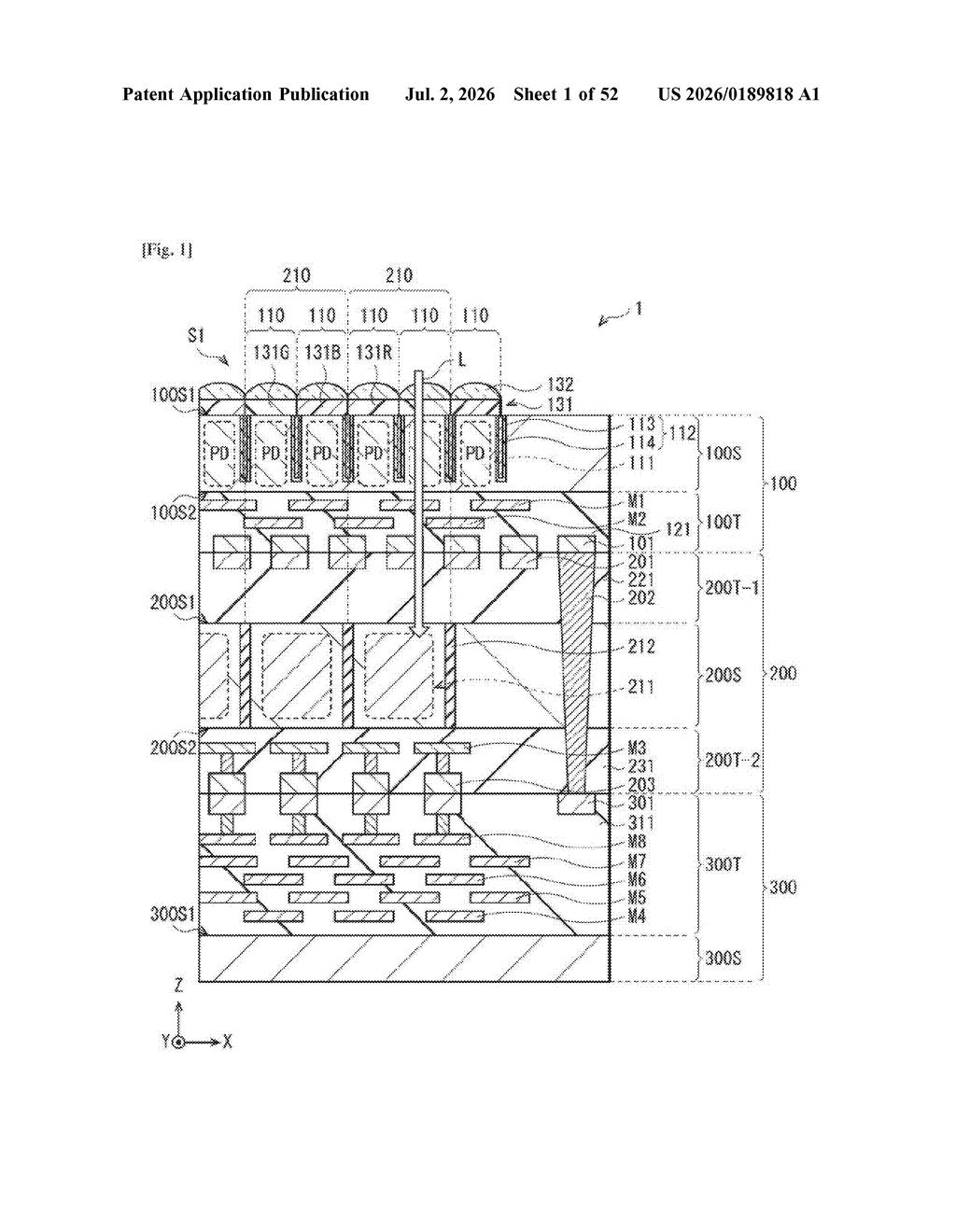
What Sony's stacked image-and-depth sensor actually does
Imagine trying to take a portrait photo where the background goes blurry, or using your phone to scan a room for AR furniture placement. Both of those tasks require your camera to know how far away everything is, not just what color it is. Right now, phones usually handle that with extra sensors or software tricks, which adds cost and complexity.
Sony's patent describes a sensor built like a three-layer sandwich. The top layer captures the regular color image you'd recognize as a photo. The middle layer captures the same incoming light but reads it differently to figure out distance. The bottom layer is a processing chip that handles both sets of data at once.
Because all three layers share the same set of lenses and are physically stacked on top of each other, the color image and the depth map are captured from exactly the same point of view, at exactly the same moment. That kind of precise alignment is hard to achieve when you rely on two separate sensors sitting side by side.
How the three substrates split light into image and depth signals
The patent describes a stacked photodetector built from three bonded silicon substrates, all sharing a single array of lenses at the top.
- First substrate (top layer): Contains standard image pixels, each with a photodiode that responds to the portion of light passing through the lens array designated for color imaging. These output the signals that become your regular photograph.
- Second substrate (middle layer): Contains depth pixels, each with a photodiode tuned to a different portion of the incoming light, including some or all of the same light the image pixels see. These output signals used to calculate how far away objects are, likely via time-of-flight or phase-detection principles.
- Third substrate (bottom layer): A dedicated logic chip with two separate processing circuits: one converts the image pixel signals into final image data, and the other converts the depth pixel signals into a depth map.
The key claim is the stacking order: lenses on top, image pixels next, depth pixels below that, and the processor at the base. Because both sensing layers look through the same lens array, there is no parallax error (the slight offset you get when two cameras sit apart from each other), which makes the depth data much easier to align with the color image.
What this means for cameras, AR, and 3D sensing
For anyone who uses portrait mode, AR apps, or 3D scanning on a phone, the quality of depth sensing directly affects how realistic the result looks. A depth sensor and a color sensor that are physically separated always see the world from slightly different angles, which forces software to compensate. A single stacked sensor eliminates that problem at the hardware level.
Sony Semiconductor Solutions is one of the largest image sensor suppliers in the world, selling chips to Apple, Samsung, and most major phone makers. A patent like this points toward next-generation sensors where high-resolution photography and accurate 3D sensing are handled by a single, compact component rather than a cluster of separate modules.
This is genuinely interesting sensor architecture from a company that supplies the camera chips inside most of the phones you've actually heard of. Stacking depth and color sensing into a single physical unit with shared optics is a real engineering goal, not a paper exercise, and Sony is well-positioned to bring it to market. Whether this specific design makes it into production is another question, but it's the kind of foundational patent worth tracking.
Get our take in your Top Stories
Liked this breakdown? Add Patentlyze as a preferred source on Google, and our plain-English take shows up more often in your Top Stories the next time Sony patent news breaks.
There are more where this came from
We read every patent application Big Tech publishes and send you the ones worth knowing. Plain English, free, every week.
Want this weekly breakdown for a company we don't cover? Patentlyze Pro →