
Samsung Patents a Camera Chip Design That Captures Sharper Photos Using Stacked Layers
Samsung has filed a patent for an image sensor that tweaks the physical construction of the transistors sitting on top of its light-capturing chip. The change is tiny, measured in hundredths of a micron, but that scale is exactly where modern image sensor performance is won or lost.
What Samsung's new image sensor gate design actually does
Think of an image sensor like a sheet of tiny light-collecting buckets. The transistors that control each bucket are incredibly small, and how they're built at the atomic level directly affects how well your camera performs in the dark or under bright light.
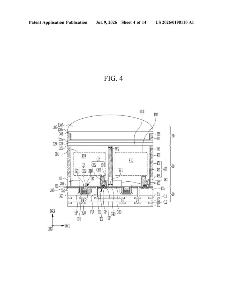
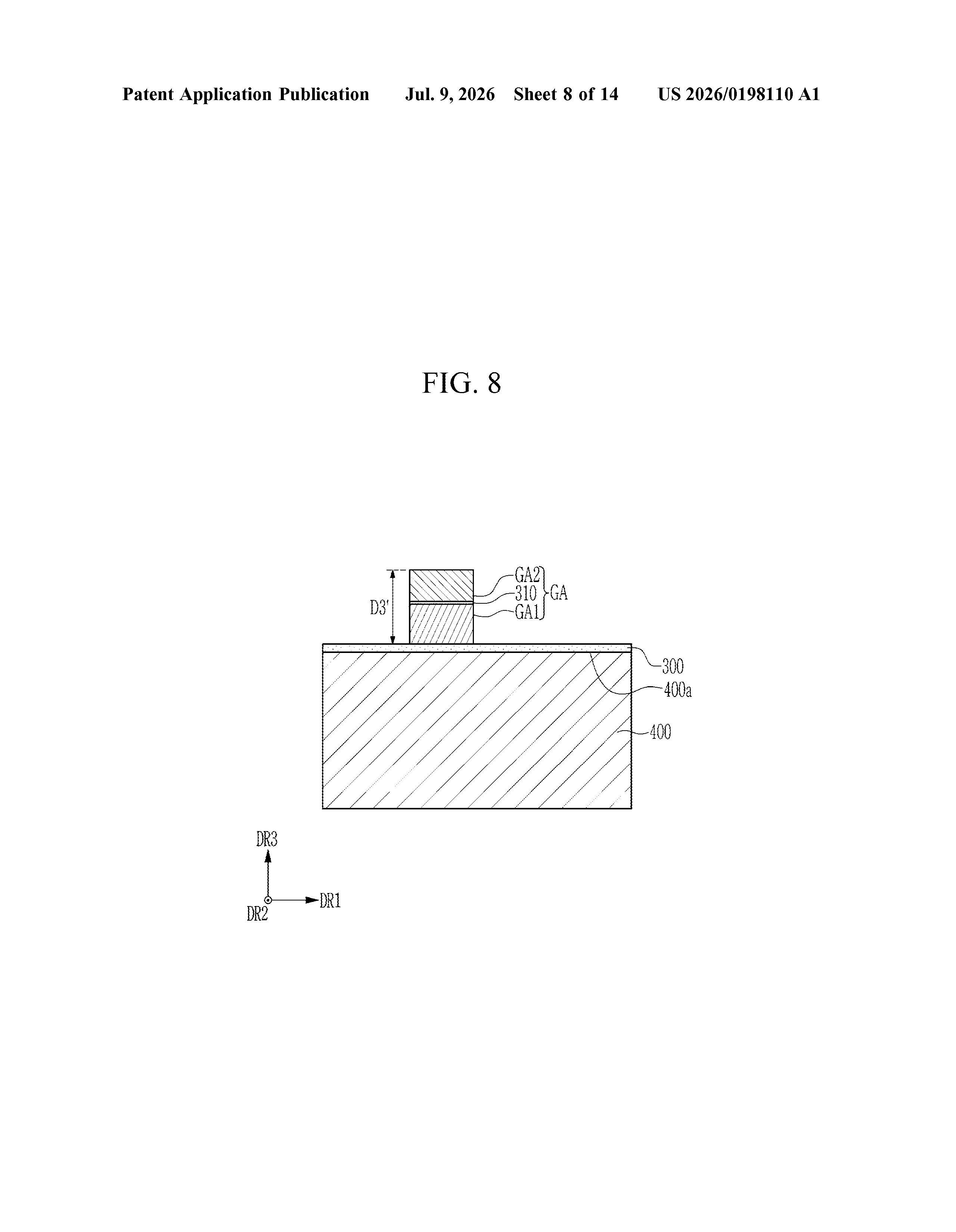
Samsung's patent describes a specific way of stacking the gate electrode (the on/off switch for each transistor) in layers, with a thin oxide film sandwiched in the middle. One transistor gets this laminated, precisely sized switch; a neighboring transistor gets a slightly sunken top surface. Together, these two design choices are meant to make the transistors behave more predictably and with less electrical noise.
For you as a phone or camera user, improvements at this level typically show up as cleaner low-light photos, more accurate colors, or the ability to cram more pixels into the same chip area without losing image quality.
How the layered gate and depressed surface work together
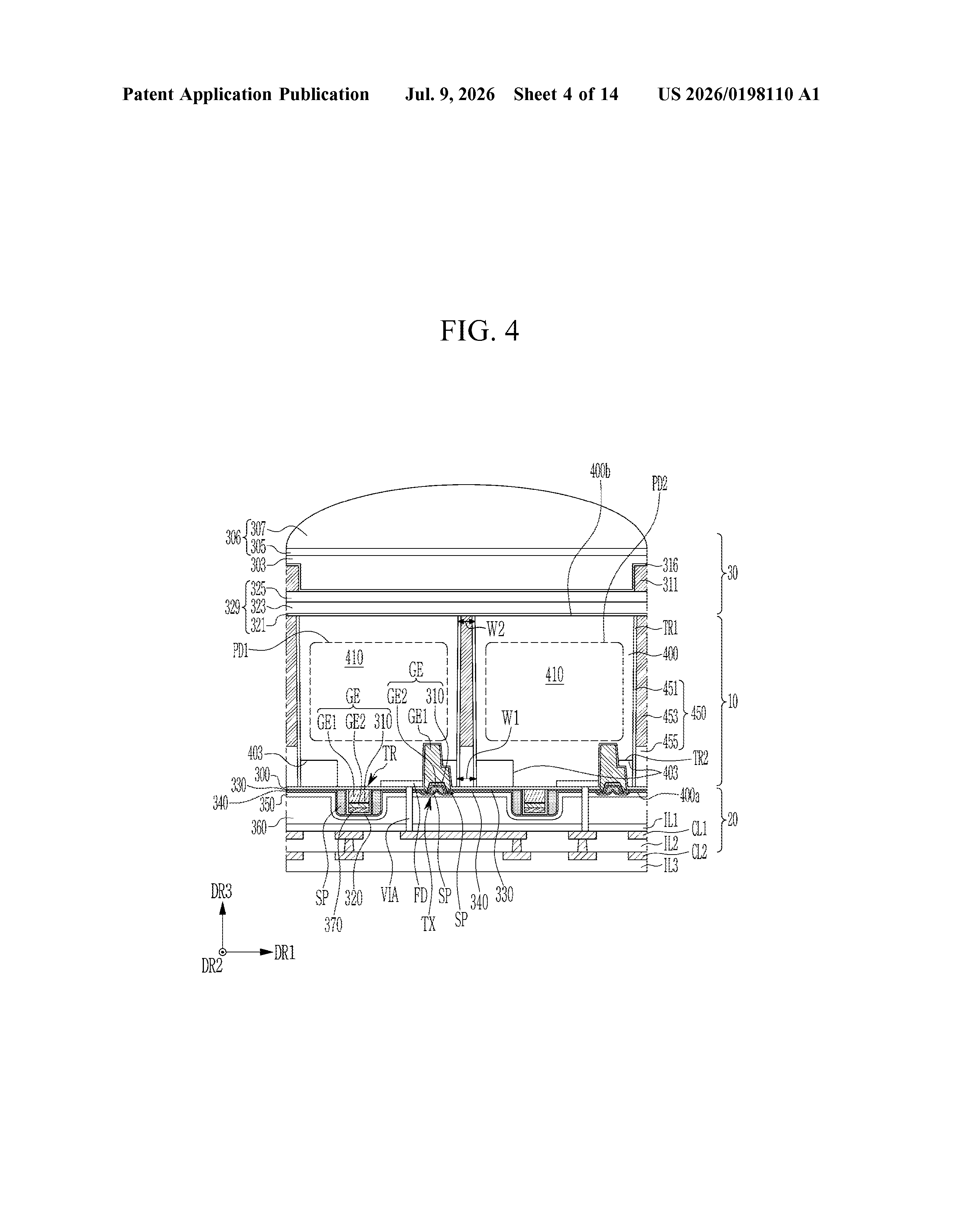
The patent describes an image sensor built on a substrate (a slice of silicon) that has two sides: one side faces the light source, and the other faces the circuitry. Two transistors sit on the circuit-facing side.
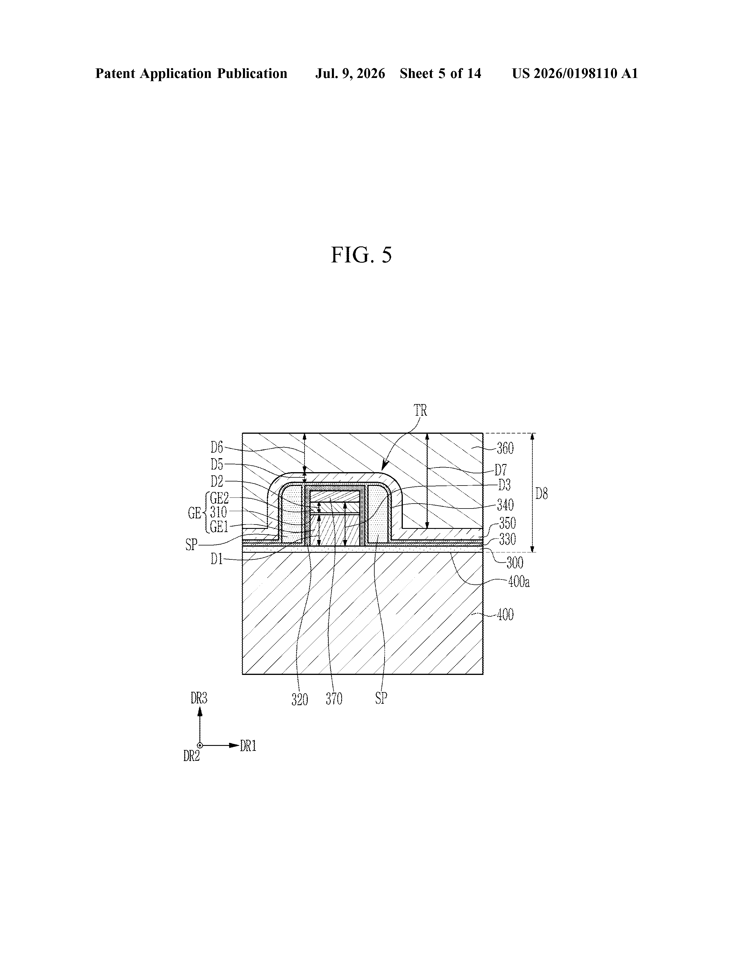
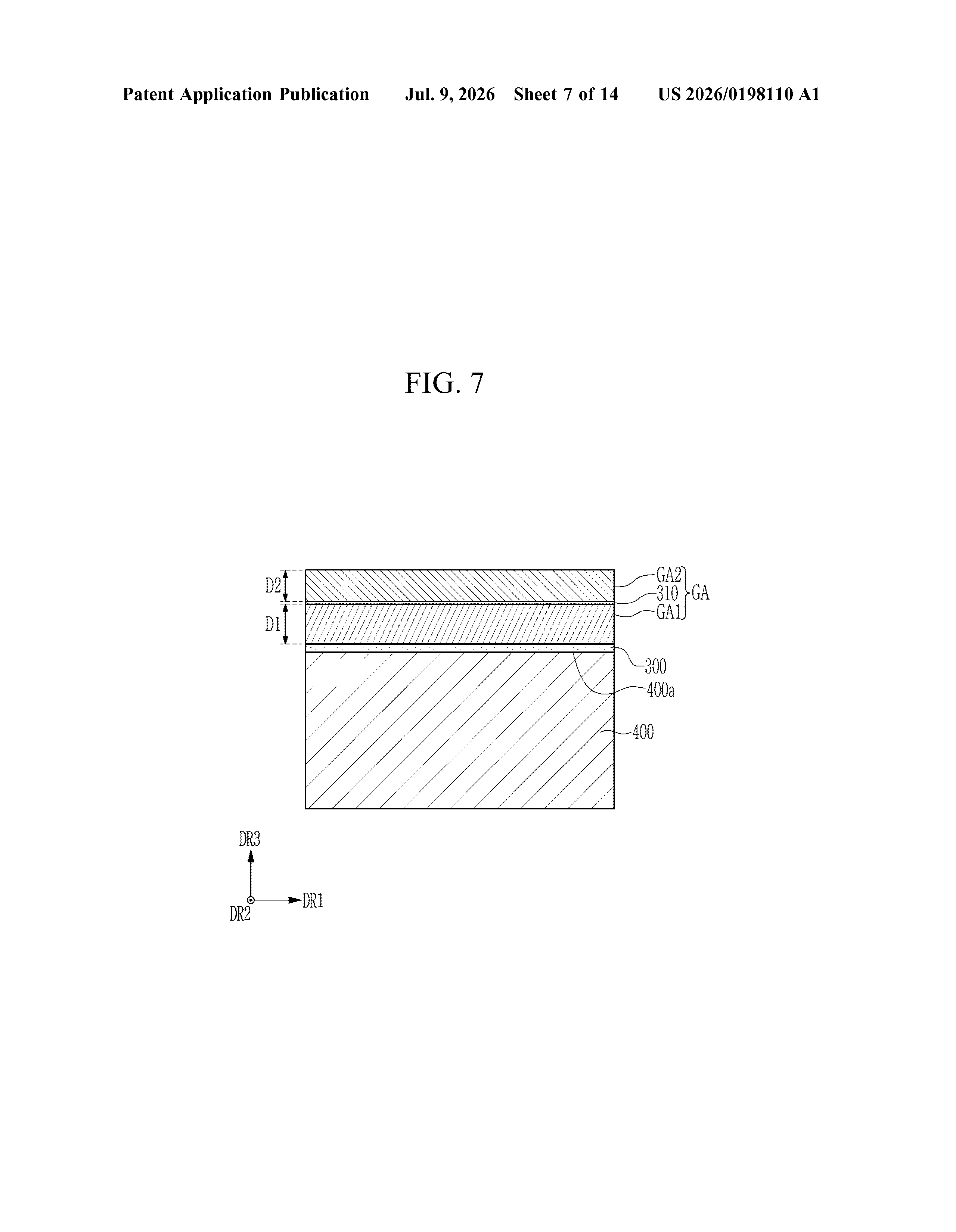
The first transistor has a gate electrode (the physical gate that switches the transistor on and off) made of three layers: a first conducting portion, a second conducting portion, and an interlayer oxide layer (a very thin insulating film) sandwiched between them. The total thickness of this gate electrode is held to a tight window of 400 to 500 angstroms (one angstrom is one ten-billionth of a meter), which is an unusually precise tolerance for this kind of structure.
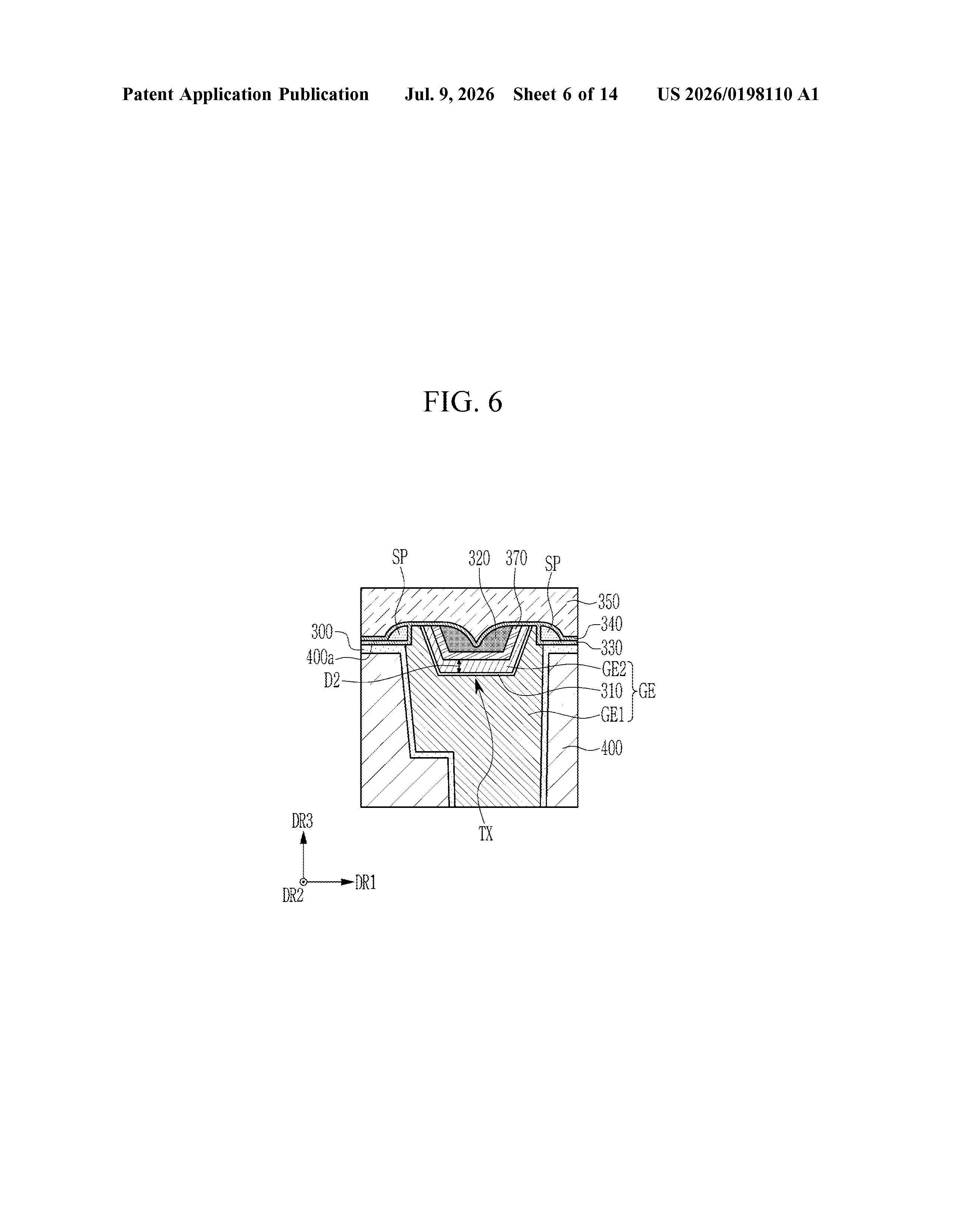
The second transistor has a different feature: the top surface of its gate electrode has a depressed region, meaning it dips inward toward the back of the chip. This kind of intentional surface geometry affects how electrical current flows and how the transistor behaves under varying charge conditions.
The combination of the layered gate on one transistor and the contoured surface on the other is the core of the invention. Both features address how charge carriers move through the transistor, which in turn affects noise, leakage current, and switching speed, all factors that shape final image quality.
What this means for Samsung's camera sensor ambitions
Image sensor performance has become one of the key battlegrounds between Samsung, Sony, and Apple's supply chain partners. Gains at the transistor-geometry level are how chipmakers push sensors further without redesigning the whole chip from scratch. A tighter gate thickness tolerance can reduce the variation between pixels, which means more consistent color and brightness across an image frame.
Samsung manufactures sensors for its own Galaxy devices and supplies chips to other brands. Patents like this one protect incremental process improvements that accumulate into a competitive edge over time. This particular filing is narrow and specific, covering one structural combination rather than a broad manufacturing method, so it reads more like a process refinement than a platform shift.
This is a quiet, incremental semiconductor process patent, the kind that rarely makes headlines but represents the real work of staying competitive in the image sensor market. It won't redefine photography, but if Samsung applies this gate geometry in production, it's the sort of change that shows up as a benchmark point in a camera review without anyone knowing why.
Get our take in your Top Stories
Liked this breakdown? Add Patentlyze as a preferred source on Google, and our plain-English take shows up more often in your Top Stories the next time Samsung patent news breaks.
There are more where this came from
We read every patent application Big Tech publishes and send you the ones worth knowing. Plain English, free, every week.
The drawings
14 drawing sheets from US 2026/0198110 A1 · click any drawing to enlarge
Want this weekly breakdown for a company we don't cover? Patentlyze Pro →