
Samsung Patents a More Efficient Way to Simulate Light on Chip Surfaces
Designing a modern computer chip requires predicting how light will behave on surfaces measured in nanometers. Samsung's new patent targets that prediction step, aiming to cut redundant calculations during the simulation.
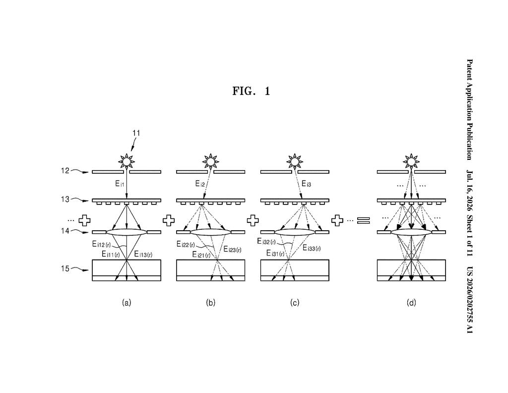
What Samsung's light simulation patent actually does
When Samsung engineers design a new chip, they run software simulations to predict how light will interact with the chip's tiny 3D structures. This matters because chipmaking uses light to etch patterns, and getting that light behavior wrong leads to defects. The simulation software has to model something called partially coherent light, which is light that isn't perfectly uniform, arriving from many different angles at once.
The problem is that running all those angle-by-angle calculations separately wastes time and memory. Samsung's patent describes a smarter bookkeeping system: as the simulation works through each angle, it checks whether it has already done a similar calculation. If it has, it reuses that result instead of starting from scratch. Results are stored in two separate memory areas depending on whether they're fresh or accumulated.
The payoff is faster, less redundant simulation runs, which could help Samsung's chip designers iterate more quickly during development without sacrificing accuracy.
How the two-storage-area calculation system works
The patent covers a simulation method for analyzing electromagnetic field characteristics (how light waves behave) when partially coherent light hits the 3D surface of a chip structure.
Partially coherent light (light with only partial phase consistency, like what real lithography equipment produces) must be broken down into individual components by incident angle before analysis can begin. The patent's method decomposes that light into separate components, each representing one incoming direction.
The core loop works like this:
- For each light component, the system checks whether this is the first calculation for that particular incoming angle.
- If yes, it runs the full calculation, normalizes the result, and saves it to a second storage area tagged to that angle.
- If no, it retrieves and reuses the prior result, adding it to an accumulated result stored in a first storage area.
- This continues until all components are processed.
The two-storage-area architecture is the key innovation: it separates the "fresh calculation" path from the "accumulation" path, avoiding redundant full computations for light components that share the same incident direction but differ in other properties.
What this means for chip manufacturing accuracy
Chip lithography simulation is one of the most computationally expensive steps in semiconductor R&D. Every time a design team wants to test a new pattern or process tweak, they may run thousands of these electromagnetic field calculations. A method that avoids repeating identical sub-calculations could meaningfully reduce simulation time at scale.
For Samsung, which operates its own foundries and designs its own chips, faster simulation tools translate directly into shorter development cycles. This patent also fits a broader industry push toward more accurate optical proximity correction, the process of pre-distorting chip designs so that light exposure produces the intended shape. More efficient simulation means engineers can test more corrections in the same time window.
This is deep infrastructure work, the kind of patent that never shows up in a product announcement but saves engineering hours across thousands of simulation runs. It's not a headline-grabbing idea, but for anyone who works on chip design software or EDA tools, the two-area storage trick is a concrete and practical contribution. Worth watching if you follow Samsung's foundry ambitions.
There are more where this came from
We read every patent application Big Tech publishes and send you the ones worth knowing. Plain English, free, every week.
Want this weekly breakdown for a company we don't cover? Patentlyze Pro →
Be the first to weigh in