
IBM Patents a Method to Untangle Complex Chip Pulses and Catch Timing Errors
Designing a chip that runs at the wrong speed is a costly mistake. IBM has filed a patent for a smarter way to check whether a chip's internal timing is correct, focusing on a type of clock signal that fires twice per cycle instead of once.
How IBM's clock-splitting method helps chip designers
Imagine a metronome that taps on both the downbeat and the upbeat, not just one or the other. Some chips use a similar trick with their internal clock signal, firing a data pulse on both the rising and falling edges of each clock tick. That's called a dual-edge pulse clock, and it lets chips pack more work into every cycle.
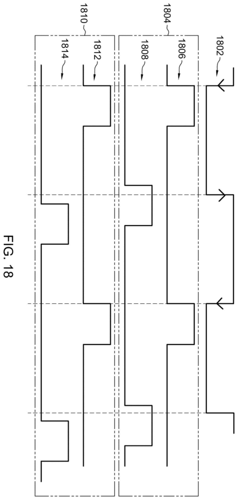
The problem is that chip design software often struggles to analyze these double-firing clocks accurately during testing. IBM's patent describes a method that takes one complex dual-edge clock and splits it into two simpler, standard clock signals for analysis purposes: one representing the pulses on the rising edge, and one representing the pulses on the falling edge.
By modeling the clock this way, timing analysis tools can check whether data is arriving where it needs to go, exactly when it needs to get there, without getting confused by the double-firing behavior. It's a behind-the-scenes fix for chip design software, not a consumer product.
How the dual-clock model captures both pulse edges
The patent covers a computer-implemented method for static timing analysis (the process of verifying that every signal in a chip design arrives at the right place within its allowed time window).
The specific problem it targets is the dual-edge pulse clock: a clock signal that generates short pulses on both the leading edge (the moment the clock signal rises from low to high) and the trailing edge (the moment it falls back to low). Standard timing tools are built around clocks that fire on only one edge, so dual-edge clocks can confuse them or require special handling that existing tools don't support well.
IBM's method works in two steps:
- Identification: The system reads the circuit's specification file and detects when a dual-edge pulse clock is derived from a base source clock.
- Modeling: It replaces that single complex clock with a pair of simpler clock signals, one to represent the leading-edge pulses and one to represent the trailing-edge pulses, so standard timing analysis tools can process each independently.
The end result is that timing analysis software can verify the chip's timing behavior correctly without needing to be rebuilt from scratch to handle dual-edge clocks.
What this means for chip design verification tools
For chip design teams, incorrect timing analysis means bugs that only show up after a chip is manufactured, which is extremely expensive to fix. Tools that can't correctly model dual-edge pulse clocks may either miss timing violations or flag false errors, both of which cost engineering time and money.
This patent is aimed squarely at electronic design automation (EDA) software, the tools companies use to verify chip designs before sending them to a fab. IBM has a long history in chip design tooling and this kind of filing is typical of incremental improvements to verification workflows. It won't appear in a consumer product, but it could surface inside IBM's internal design tools or in commercial EDA software.
This is a narrow, incremental fix to a specific problem in chip timing analysis software. It's not a broad platform play or a signal of strategic direction. If you work in EDA or chip verification, it's worth a look; if you don't, you can safely skip it.
Get our take in your Top Stories
Liked this breakdown? Add Patentlyze as a preferred source on Google, and our plain-English take shows up more often in your Top Stories the next time IBM patent news breaks.
There are more where this came from
We read every patent application Big Tech publishes and send you the ones worth knowing. Plain English, free, every week.
The drawings
22 drawing sheets from US 2026/0212098 A1 · click any drawing to enlarge


Show the other 14 sheets


Want this weekly breakdown for a company we don't cover? Patentlyze Pro →