Samsung Patents a Vertical Transistor Design That Grows Its Own Channels
Samsung is filing patents on a vertical transistor architecture where the semiconductor channel material is grown directly out of the electrode beneath it — a fabrication shortcut that could simplify how ultra-dense chips are built.
How Samsung's vertical transistor builds itself from the bottom up
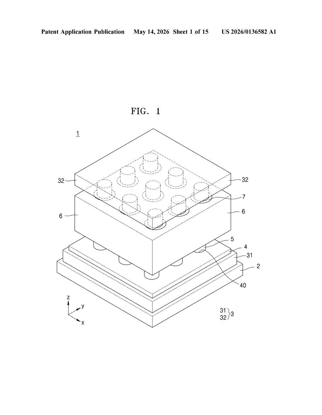
Imagine stacking the layers of a chip like a tiny skyscraper instead of spreading them flat across a floor. That's the basic idea behind a vertical transistor: instead of laying transistors side by side on a flat surface, you build them upward. Samsung's patent describes a device that does exactly this.
The clever part is where the channel material comes from. The bottom electrode is made of a transition metal (think molybdenum or tungsten), and the channels — the tiny conductive wires that the transistor switches on and off — are grown directly out of that same electrode. A patterned mask layer controls exactly where those channels sprout up, like a stencil guiding seedlings through holes in a mat.
The gate electrode then wraps around each channel, and the top electrode caps them off. The result is a compact, self-aligned structure where the chemistry of the channel and its source electrode are intentionally linked — which can mean fewer fabrication steps and tighter control over electrical behavior.
How the TMD channels grow from the electrode layer
The patent describes a vertical structure semiconductor device built around transition metal dichalcogenide (TMD) channels — materials like MoS₂ or WS₂ that have attracted intense research interest because they can be made just a few atoms thick while remaining electrically active.
Here's how the stack is organized:
- A first electrode layer containing a transition metal element (e.g., molybdenum) sits at the bottom.
- A mask layer made of metal oxide sits on top of that electrode, with patterned openings called channel growth regions — essentially, holes that define where channels will form.
- TMD channels grow upward through those openings, with their bottom ends rooted in the exposed electrode surface. Crucially, the TMD incorporates the same transition metal as the electrode below, suggesting epitaxial or chemically continuous growth.
- A gate insulating layer and a first gate electrode wrap around each channel, giving the gate a cylindrical, all-around geometry — which is excellent for electrostatic control.
- A second electrode layer contacts the tops of all the channels.
The all-around gate geometry (sometimes called a gate-all-around or GAA structure) means the gate can switch the channel on and off more efficiently than a planar gate, reducing leakage current. The shared transition metal between electrode and channel is the structural novelty — it implies the channels may be grown in situ from the electrode, potentially simplifying alignment.
What vertical transistors mean for next-gen memory and logic chips
As planar transistor scaling hits physical limits, the semiconductor industry is increasingly turning to 3D architectures — stacking transistors vertically to keep packing more compute into the same footprint. Samsung's NAND flash memory already uses vertical stacking aggressively, and this patent extends that thinking to the transistor channel itself.
For memory and logic applications, a vertical TMD transistor with a gate-all-around structure could offer better switching performance at smaller dimensions than silicon-based alternatives. If the in-situ channel growth process is manufacturable at scale, it could reduce the number of deposition and alignment steps needed — which translates directly to yield and cost. This is infrastructure-level R&D, but it maps clearly onto Samsung's roadmap for both advanced DRAM and next-generation logic nodes.
This is serious materials-engineering work, not a concept patent. The specific detail that the TMD channel shares its transition metal with the bottom electrode suggests Samsung's process team has a real growth chemistry in mind, not just a wishful architecture diagram. It won't make headlines at a product launch, but patents like this are exactly the kind of foundational IP that determines who can manufacture sub-2nm transistors five years from now.
Get one Big Tech patent every Sunday
Plain English, intelligent commentary, no hype. Free.
Editorial commentary on a publicly published patent application. Not legal advice.