Samsung Patents a Two-Level Gate Wiring Layout for Semiconductor Devices
As chips shrink to atomic scales, routing electrical connections between transistors becomes a puzzle in three dimensions. Samsung's latest patent tackles exactly that — a precise two-level wiring scheme for connecting gate structures across adjacent active regions on a chip.
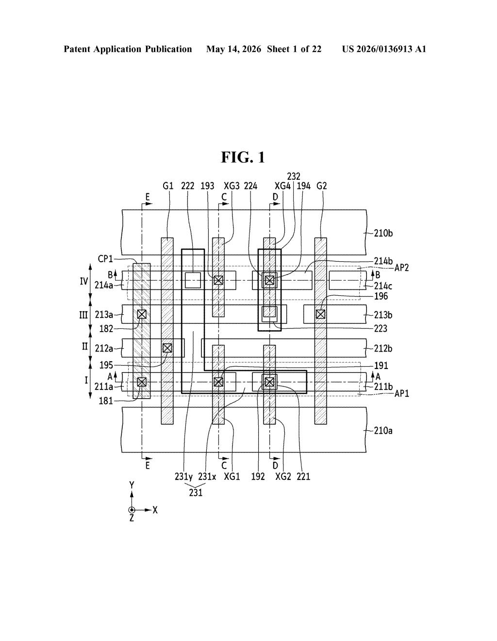
What Samsung's stacked chip wiring layout actually does
Imagine a city grid where streets run both horizontally and vertically, and some roads pass over others on elevated bridges. That's roughly what's happening inside a modern chip — electrical signals need to travel between transistors without crashing into each other.
Samsung's patent describes a specific way to organize those "roads" across two stacked levels of wiring. On the lower level, individual wires connect directly to transistor gate structures. On the upper level, specially shaped wires act like bridges, linking gates on one row of transistors to gates on a neighboring row. One of those upper wires even has an L-shaped design to reach across in two directions at once.
The result is a compact, efficient wiring layout that lets the chip designer hook up multiple gates with fewer layers and less wasted space — which matters enormously when you're trying to fit billions of transistors onto a fingernail-sized piece of silicon.
How Samsung's two-level wiring connects gate structures
The patent defines a semiconductor device with two sets of active patterns — think of these as parallel rows of transistors — each intersected by two gate structures. That gives you four gates total, spread across two rows.
First-level wiring (the lower metal layer) includes five wiring patterns, each running in the same direction as the active rows. The first four connect one-to-one to the four gate structures. The fifth sits in between the second and fourth wiring patterns and acts as an intermediary.
Second-level wiring (the upper metal layer, sitting above the first) contains two key patterns:
- A first upper wiring pattern with an L-shape — one segment runs parallel to the active rows and connects to the second gate's wire below, while a perpendicular arm reaches across to connect to the third gate's wire on the neighboring row.
- A second upper wiring pattern that runs perpendicular to the active rows and bridges the fourth gate's wire to the fifth (intermediary) wire.
Finally, the fifth lower wiring pattern is also electrically tied back to the first gate's wire, closing a loop across the layout. The net effect is a cross-connected gate network achieved with just two compact wiring levels — minimizing the vertical stack height while still enabling complex inter-gate routing.
What this means for Samsung's advanced chip scaling
In advanced logic chips — especially at 3nm and below — every additional metal routing layer adds cost, complexity, and yield risk. A scheme that cross-connects gate structures across neighboring active rows using only two levels of metal is genuinely useful for standard cell design, where circuit blocks are repeated millions of times across a chip.
For Samsung, which competes directly with TSMC and Intel Foundry on leading-edge process nodes, innovations in local interconnect and gate routing can translate into denser standard cells, lower power, and better performance. You may never see this patent cited in a product announcement, but layouts like this quietly underpin the transistor count claims Samsung makes when it launches a new process node.
This is deep semiconductor plumbing — not flashy, but exactly the kind of layout IP that matters in a foundry war. Samsung filing precise gate-routing geometry patents signals active R&D investment in standard cell architecture for advanced nodes. It's worth filing away if you track Samsung's foundry roadmap.
Get one Big Tech patent every Sunday
Plain English, intelligent commentary, no hype. Free.
Editorial commentary on a publicly published patent application. Not legal advice.