Samsung Patents a Multi-Grating Overlay Measurement Method for Chip Fabrication
Getting semiconductor layers to line up within a few nanometers across an entire wafer is one of the hardest problems in chip manufacturing. Samsung's new patent tries to make that alignment measurement more reliable by averaging signals from multiple reference gratings buried at different depths.
What Samsung's stacked grating alignment trick actually does
Imagine you're trying to stack hundreds of ultra-thin transparent sheets on top of each other, each printed with a tiny circuit pattern, and every sheet has to line up with the ones below it to within a fraction of a human hair's width. That's essentially what happens when a chip fab builds a modern processor — layer by layer, with each new layer needing to be precisely registered to everything below it.
The tricky part is measuring that alignment. Fabs use tiny reference patterns called metrology marks — think of them like registration crosses on a printing press — etched into the wafer. The problem is that a single reference mark can give a noisy or misleading reading if the layer it lives on has imperfections.
Samsung's patent describes a method where two sets of reference marks, deposited at different times and possibly different depths, are measured together and their readings averaged into a single combined value. A new top-layer mark is then compared against that averaged baseline. The idea is that by blending two independent reference signals, you cancel out the noise from either one alone and get a more trustworthy alignment number.
How Samsung averages bottom gratings to anchor overlay measurement
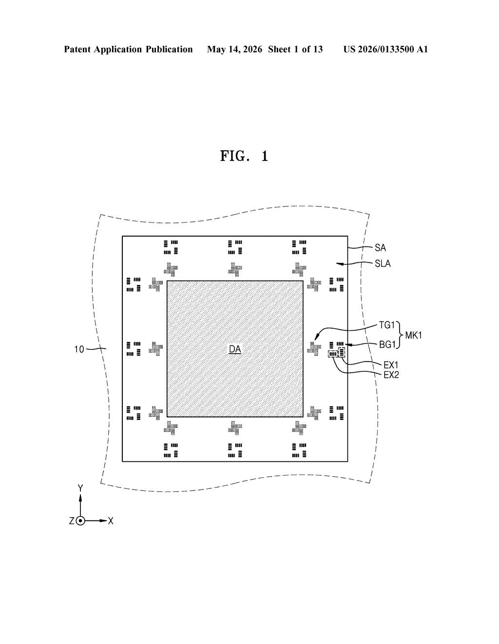
The patent describes a photolithography overlay measurement process built around a concept Samsung calls a bottom grating integrated measurement value. Here's how it breaks down:
- Two bottom gratings are formed at different time instances — meaning they were deposited in separate process steps, potentially at different vertical levels within the chip stack. Each grating is a set of tiny periodic structures (think micro-scale ruled lines) that an optical metrology tool can read.
- Each grating is measured independently for its alignment offset — how far it has drifted from where it should be. These two readings are then averaged into a single integrated measurement value.
- A top grating is then deposited at a higher vertical level, and its overlay error (how much it has shifted relative to the layers below) is calculated using both its own optical measurement and the pre-computed bottom average.
The core insight is that each grating layer may carry its own process-induced distortion — stress, chemical-mechanical planarization artifacts, or etch bias — that makes it an imperfect standalone reference. By averaging two independent bottom references formed at different process steps, Samsung reduces the influence of any single layer's idiosyncrasies. The method is also designed to handle cases where the two bottom gratings sit at the same vertical level or at different ones, giving it flexibility across different device architectures.
What this means for Samsung's leading-edge chip yields
Overlay error — the misalignment between successive patterning layers — is one of the primary yield killers in advanced logic and memory manufacturing. At 3nm and below, even a few nanometers of drift can cause a transistor gate to miss its contact, turning a working chip into scrap. Better overlay measurement directly translates to higher yield and lower cost per chip.
For Samsung, which competes with TSMC and SK Hynix across both logic and DRAM/NAND, incremental improvements in metrology are a real competitive lever — not a footnote. This patent doesn't describe a new sensor or a new light source; it describes a smarter measurement protocol that could be layered on top of existing equipment. That makes it relatively low-cost to adopt and potentially high-impact on the fab floor.
This is a quiet but genuinely useful patent — not a flashy AI play, but the kind of process-engineering detail that separates fabs that yield 60% from fabs that yield 80%. The averaging-of-gratings idea is elegant precisely because it doesn't require new hardware, just a smarter measurement recipe. Don't expect a press release, but do expect something like this to quietly appear in Samsung's advanced node process flows.
Get one Big Tech patent every Sunday
Plain English, intelligent commentary, no hype. Free.
Editorial commentary on a publicly published patent application. Not legal advice.