
Samsung Patents a Wafer Inspection System That Tells AI Where Every Chip Sits
When you photograph a circular wafer packed with hundreds of identical chips, the AI inspecting it has no idea which chip is which, unless you tell it. Samsung's new patent solves that orientation problem using a coordinate system borrowed from geometry class.
How Samsung's wafer-scanning AI finds its bearings
A factory camera photographs a silicon wafer covered in hundreds of tiny chips arranged in a circular grid. The photo lands on an AI, but the AI sees a flat image with no built-in sense of where each chip sits relative to the center or the edge.
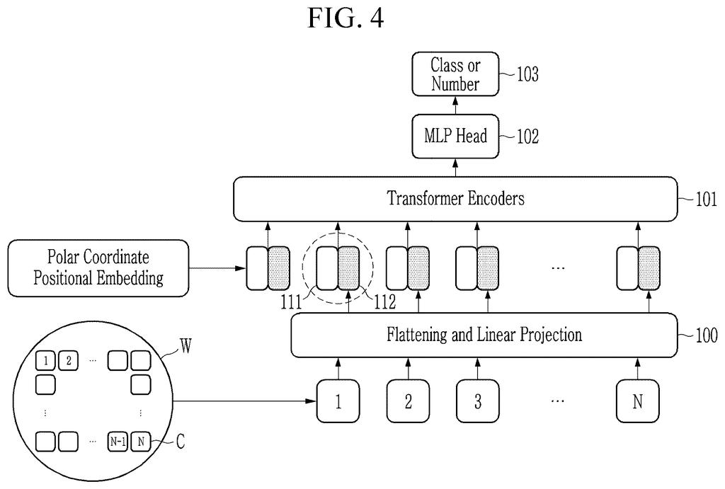
Samsung's approach gives the AI a map. Before the image is analyzed, the system reads each chip's position in polar coordinates (think: how far from the center, and at what angle, like a clock hand pointing to a chip). Those coordinates are turned into small numerical tags and attached to the AI's representation of each chip, so the model always knows where on the wafer it's looking.
The practical payoff is more accurate inspection. Defects on the edge of a wafer behave differently from defects near the center, and an AI that knows the difference can flag problems with more confidence than one treating every chip as if it were identical.
… extracting respective polar coordinates of a chip-specific positions from within the image data of the wafer; generating a plurality of positional embeddings from a plurality of polar coordinates; and combining the plurality of positional embeddings and the plurality of chip embeddings, respectively to input the combination into a neural network.
Translation: The system maps the exact circular location of each chip on the wafer and feeds that data into an AI model.
How polar coordinates become positional embeddings
The patent describes a five-step pipeline that prepares wafer image data for analysis by a neural network:
- Chip separation: The full wafer image is sliced into individual chip images, one per chip on the wafer.
- Chip embeddings: Each chip image is flattened (its pixel grid is unrolled into a single row of numbers) and passed through a linear projection (a learned mathematical filter) to produce a compact numerical summary called an embedding.
- Polar coordinate extraction: Rather than recording each chip's location as an X-Y grid address, the system records it as a distance from the wafer's center and an angle, forming a polar coordinate. Wafers are circular, so this geometry fits naturally.
- Positional embeddings: The polar coordinates are converted into their own set of numerical summaries, called positional embeddings, that the neural network can read alongside the image data.
- Combination and input: Each chip's image embedding and its positional embedding are merged and fed together into the neural network for classification or defect detection.
The positional encoding step is the key contribution. Standard vision transformers (a type of neural network that processes images as sequences of patches) typically use simple row-and-column grid positions. For a round wafer, that grid is a poor fit. Polar coordinates preserve the radial symmetry of the wafer layout, so the model receives location information in a form that matches the physical reality of how chips are arranged.
… generating chip-specific data for respective chips by separating image data including a plurality of chips formed on a wafer, generating a plurality of chip embeddings by performing flattening and linear projection on the chip-specific data …
Translation: The software isolates individual chips from a larger wafer image and converts their visual features into a digital format.
What this means for AI-driven chip manufacturing
Semiconductor inspection is one of the most quality-sensitive steps in chip manufacturing. A single undetected defect pattern can mean scrapping an entire wafer or, worse, shipping faulty dies. AI-driven inspection promises faster throughput than human review, but only if the model can distinguish a center-of-wafer defect cluster from an edge-of-wafer one, two patterns that have very different root causes and call for different process fixes.
Samsung's filing is a targeted engineering fix for a gap in how vision models handle circular layouts, and it sits in a growing body of new Big Tech patents applying positional-encoding techniques to semiconductor manufacturing rather than natural-language or general-image tasks. Whether this approach shows up in Samsung's fab tooling or stays as foundational IP is an open question, but the problem it solves is real and the inspection market is large.
The design trade here is worth naming: polar coordinates are a better geometric fit for a round wafer, but they introduce a coordinate system that most off-the-shelf neural network tooling does not natively expect. Every downstream fine-tuning step, every attempt to transfer a pretrained vision model to this task, now has to bridge that gap. The benefit is better spatial context for the model; the cost is added complexity in training pipelines and potential friction when integrating with standard computer-vision frameworks. That trade reads as reasonable for a company running its own fabs, where the engineering overhead is absorbed internally and the accuracy gain matters more than interoperability with generic tools.
There are more where this came from
We read every patent application Big Tech publishes and send you the ones worth knowing. Plain English, free, every week.
The drawings
10 drawing sheets from US 2026/0237056 A1 · click any drawing to enlarge


Want this weekly breakdown for a company we don't cover? Patentlyze Pro →
Be the first to weigh in