
Sony Patents a Triple-Layer Camera Chip That Runs Two Sensors at Once
Sony's new patent describes a camera chip built from three stacked silicon layers, each with a distinct job: one captures light, one detects motion changes, and one converts everything into digital data. The goal is to make all three layers fit together without wasting a single millimeter of chip area.
What Sony's stacked three-chip camera sensor actually does
You're recording a fast-moving scene with your camera and two things need to happen at the same time: the sensor has to capture a sharp, full-resolution frame and instantly flag anything that just moved. Most chips struggle to do both efficiently because they're trying to cram two very different jobs onto the same piece of silicon.
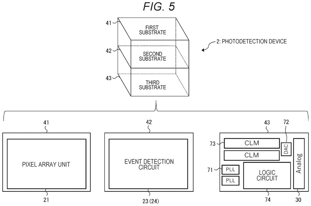
Sony's patent describes a sensor built from three separate chips bonded together in a stack. The bottom layer captures light from two sets of pixels. The middle layer watches for sudden changes in brightness (the kind of thing that tells a camera "something moved"). The top layer handles the number-crunching that turns raw light data into a proper digital image. Each layer only does its own job, so none of them wastes space accommodating the other two.
The practical payoff is a sensor that can shoot normal video and react to fast motion events at the same time, without one task slowing down the other. That combination is useful anywhere a camera needs both a clean image record and split-second motion awareness.
… a first signal processing circuit that performs signal processing by performing analog-to-digital conversion on a plurality of pixel signals according to the amount of incident light on a basis of the charges accumulated in the plurality of first photoelectric conversion elements …
Translation: The chip converts light into digital data using one set of sensors to create standard images.
How the three substrates divide the sensing workload
The patent describes a photodetection device built by physically bonding three semiconductor substrates on top of each other.
- First substrate (bottom): holds two sets of photoelectric conversion elements (the tiny structures that turn incoming light into electrical charge). One set feeds the normal image pipeline; the other feeds a separate motion-detection circuit.
- Second substrate (middle): contains an event detection circuit, which watches the charge from the second set of pixels and generates an "event signal" whenever the brightness at any point changes by a meaningful amount. This is similar to how event cameras work: instead of capturing every frame at a fixed rate, they only note what changed and when, which is extremely fast and power-efficient.
- Third substrate (top): holds the analog-to-digital conversion circuit (the circuitry that translates the continuous electrical signal from the first pixel set into discrete numbers a processor can use), producing conventional pixel-by-pixel image data.
The key engineering claim is about area efficiency. Because each substrate handles only one type of circuit, the designers can size each layer to match exactly what that layer needs, preventing empty silicon from appearing in any of the three tiers. The layers communicate through vertical electrical connections between the bonded chips.
A size of stacked chips can be optimized by preventing a useless space from being generated in each layer of the stacked chips.
Translation: Sony designed this three-layer chip to be as compact as possible by eliminating empty space between the layers.
What this means for cameras that need speed and detail together
Cameras that need to track fast objects (think autonomous vehicles, robotics, high-speed industrial inspection, or high-end smartphones in sport mode) currently have to choose between conventional image quality and event-based speed. A chip that handles both in hardware, on a single compact stack, removes that tradeoff at the sensor level rather than pushing it onto software.
Sony Semiconductor Solutions is one of the world's dominant image sensor suppliers, so a structural change to how they stack chip layers has downstream effects on every device that uses their sensors. The three-substrate approach described here is the kind of incremental-but-load-bearing architecture patent that shapes product lines for years, and it sits alongside a growing body of new tech patents in stacked image-sensor design that signal where camera silicon is heading.
Sony's 336th filing among the patents we've tracked since May includes earlier work on seeing through glass and fixing avatar elbows in VR, all part of our Sony coverage.
Putting two sensing systems on separate chips stacked together is clever, but it creates a real problem. The tiny electrical connections linking those stacked chips are extremely difficult to make reliably in a factory, and each one is a new way for the product to break.
The patent openly admits the whole design exists to avoid wasted space on each chip layer. The designers knew the manufacturing headache was coming and accepted it as the price of a smaller, more capable sensor.
That trade makes sense for high-end devices where size and dual sensing are mandatory. For cheap, mass-market products, this design will likely stay out of reach for years.
There are more where this came from
We read every patent application Big Tech publishes and send you the ones worth knowing. Plain English, free, every week.
The drawings
26 drawing sheets from US 2026/0247047 A1 · click any drawing to enlarge


Want this weekly breakdown for a company we don't cover? Patentlyze Pro →
Be the first to weigh in