
Sony Patents Factory Sensor That Spots Tiny Cracks the Moment They Appear
Sony has filed a patent for a surface-inspection system that replaces slow, frame-by-frame cameras with a sensor that only reacts when something changes, potentially catching tiny cracks the moment they appear.
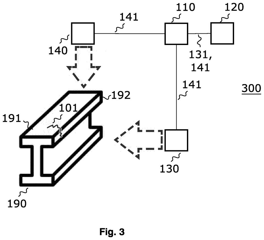
How Sony's crack-detection camera system actually works
Imagine you're running a factory line that stamps out thousands of metal parts per hour. Your job is to catch any crack before a flawed part ships, but a regular camera shoots the same full picture over and over, making your inspection software sift through enormous amounts of redundant data just to spot one tiny flaw.
Sony's patent describes a different kind of camera called an event-based vision sensor. Instead of capturing full frames at fixed intervals, each pixel in this sensor fires independently the moment it detects a change in light. That means the camera is essentially silent when nothing is happening, and then suddenly very loud when something like a crack edge passes under the light.
A processing system watches that stream of pixel-level "events" and uses it to decide whether a crack is present on the surface being scanned. Because you're only processing the pixels that actually changed, the whole system can react much faster and with far less wasted computation than a conventional machine-vision camera.
interface circuitry configured to receive an image stream of an event-based vision sensor, wherein the image stream comprises a plurality of images for consecutive time instants during the capture of a surface of the object …
Translation: The system uses a specialized camera that records a rapid series of images to track changes on a surface over time.
Inside Sony's event-pixel image stream and crack classifier
The patent centers on two main hardware blocks: interface circuitry that ingests the data stream from an event-based vision sensor, and processing circuitry that analyzes that stream to flag cracks.
An event-based vision sensor (sometimes called a neuromorphic camera) works very differently from a conventional camera. Instead of capturing a full image grid at regular clock ticks, each pixel reports independently and only when the local brightness crosses a threshold. The result is a timestamped list of "which pixel changed and when" rather than a stack of full frames.
The patent's claim covers building an image representation from that stream by organizing pixels across consecutive time instants, essentially reconstructing mini-frames that encode motion and edge information without the blank data that floods a normal frame. The processing circuitry then reads those reconstructed images to determine whether a crack is present.
The filing also covers a companion method for training a machine-learning model on this kind of data, suggesting Sony intends the crack-detection decision to be made by a neural network rather than hand-coded rules. That matters because cracks can look very different depending on material, lighting angle, and scan speed.
… processing circuitry configured to determine the presence of a crack on the surface of the object based on the image stream.
Translation: The computer analyzes the visual data to automatically detect if there is a crack on the object being scanned.
What this means for factory inspection and Sony's sensor business
For manufacturers, the appeal is speed and sensitivity. A standard machine-vision camera has to process every pixel in every frame, which creates a ceiling on how fast the production line can move. An event-based sensor sidesteps that bottleneck because it only generates data when something actually changes, so a crack edge, which is a sharp transition in brightness, produces a dense burst of events while an intact surface stays mostly quiet. That asymmetry is exactly what you want in a defect-detection pipeline.
Sony already makes image sensors used throughout the industrial and consumer markets, so this patent sits in a business area the company knows well. The specific focus on surface crack detection points toward quality-control automation in manufacturing, where faster and more reliable inspection has direct dollar value. Sony's sensor ambitions in machine vision are part of a wider wave of new Big Tech patents aimed at pushing AI-driven inspection deeper into factory floors.
Sony's 361st filing among the patents we've tracked since May joins earlier work like a Wi-Fi packet filter and a camera noise fix in our Sony coverage.
The problem with these new sensors is that they are much harder to use than a regular camera. Instead of taking neat pictures, they only record the moment something moves, sending out a scattered stream of signals that no existing software was built to handle.
Sony is betting the speed boost is worth rebuilding all that software from the ground up. For factories churning out thousands of parts a day, that bet probably pays off. But the real question is simpler and scarier: can the system be trained well enough that it never misses a crack in a load-bearing part? One missed defect costs far more than a slow inspection line.
Get our take in your Top Stories
Liked this breakdown? Add Patentlyze as a preferred source on Google, and our plain-English take shows up more often in your Top Stories the next time Sony patent news breaks.
There are more where this came from
We read every patent application Big Tech publishes and send you the ones worth knowing. Plain English, free, every week.
The drawings
12 drawing sheets from US 2026/0245197 A1 · click any drawing to enlarge


Want this weekly breakdown for a company we don't cover? Patentlyze Pro →
Be the first to weigh in