
Samsung Patents a Chip That Does Math Where It Stores Data
Every time a chip does a calculation, it has to fetch numbers from memory and haul them back. Samsung's new patent skips that trip entirely by doing the math where the data already lives.
What Samsung's in-memory computing patent actually does
Ever wondered why your phone gets hot running AI apps, even simple ones? A big part of the answer is that modern chips waste enormous energy just moving numbers around. The processor sits on one part of the board, memory sits on another, and data shuttles back and forth millions of times per second.
Samsung's patent describes a processing element that lives inside the memory itself. Instead of sending numbers out to a separate processor, the memory chip does the multiplication and addition right where the data is stored. The result comes out the other side without the data ever leaving home.
That kind of setup matters most for AI workloads, which are basically enormous piles of multiply-and-add operations done over and over. Cutting the travel time for those numbers could mean faster results, cooler devices, and longer battery life.
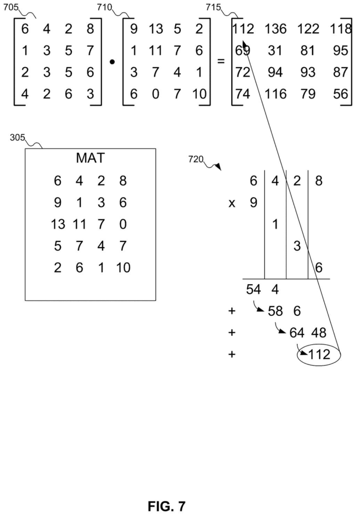
a memory array to store at least a first value and a second value; a first circuit to access the first value and the second value from the memory array; and a multiply and accumulate (MAC) circuit to process the first value and the second value to produce a third value, wherein the processing element is within a memory.
Translation: The chip performs calculations directly inside the memory storage area instead of moving data to a separate processor.
How the MAC circuit works inside the memory array
The patent describes a processing element built directly into a memory chip. It has three main parts:
- A memory array that stores the input values (think of it as a tiny spreadsheet inside the chip)
- A first circuit that reads the values out of that array
- A multiply and accumulate (MAC) circuit that does the actual math
The MAC operation (multiply and accumulate) is the fundamental building block of AI inference. When a neural network processes an image or a sentence, it is running millions of MACs: multiply two numbers, add the result to a running total, repeat. Traditionally this happens in a separate processor core, which means the memory just stores numbers and waits to be asked.
Here, the MAC circuit is inside the memory. The values never leave. The third value produced by the MAC is a result that can then feed the next layer of computation. The patent frames the whole unit as a self-contained processing element that happens to be physically located within a memory device, which is the core claim of the processing-in-memory (PIM) architecture.
The processing element may also include a multiply and accumulate (MAC) circuit to process the first value and the second value to produce a third value. The processing element may be part of a memory.
Translation: This design embeds a specialized math engine inside the memory hardware to speed up data processing.
What this means for AI chips and power efficiency
The bottleneck between memory and processor, sometimes called the memory wall, has been a known drag on computing performance for decades. It hits hardest in AI workloads, where the ratio of math operations to data movement is sky-high. A chip that collapses that distance even partially can reduce power draw and improve throughput without asking software to change at all.
For Samsung, which makes both memory chips and system chips for devices ranging from phones to data-center servers, this kind of architecture sits squarely at the intersection of its two core businesses. The latest Big Tech patents in the memory and AI-chip space show a broad industry push to rethink where computation happens, and this filing adds Samsung's formal stake to that effort.
Samsung's 40th filing we've tracked in our AI chip wars watch since June builds on earlier work like one cutting wireless interference and one translating memory requests.
Moving data back and forth between a chip's memory and its calculating core burns a huge amount of power. In a data center handling thousands of AI tasks every second, that waste adds up fast. Putting the calculator directly inside the memory attacks that problem at the root, which is a sensible fix for a real cost.
The patent stakes out a wide claim but skips the fine details. How well this actually works in practice will depend on specifics we have not seen yet.
Get our take in your Top Stories
Liked this breakdown? Add Patentlyze as a preferred source on Google, and our plain-English take shows up more often in your Top Stories the next time Samsung patent news breaks.
There are more where this came from
We read every patent application Big Tech publishes and send you the ones worth knowing. Plain English, free, every week.
The drawings
22 drawing sheets from US 2026/0245613 A1 · click any drawing to enlarge


Want this weekly breakdown for a company we don't cover? Patentlyze Pro →
Be the first to weigh in