
Samsung Files Patent for Mobile Memory That Compresses Data While Saving Battery Life
Moving data from memory to a processor burns power and slows things down. Samsung's new patent describes a way to decompress and crunch that data before it ever leaves the memory chip.
What Samsung's in-memory decompression actually does
A mobile chip stares at a pile of compressed data sitting in RAM, waiting to process it. To do anything useful, it normally has to ship that data across a power-hungry data bus to a separate processor, decompress it there, and then compute. Every trip costs time and battery.
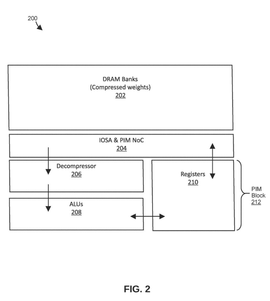
Samsung's patent describes a different approach: do the decompression work inside the memory chip, right next to where the data is stored. The chip reads compressed data from its RAM banks, splits it into chunks, and hands each chunk to a small decompressor living in the memory itself. Once decompressed, the data goes straight to a tiny calculator unit, also inside the memory, for processing.
The result is that less raw data has to travel across the chip at all times, because it stays compressed until the last possible moment. For your phone, that could mean AI tasks and other heavy workloads running faster while using less power.
obtaining, by an input/output sense amplifier (IOSA) from an associated random access memory (RAM) bank, compressed data; sending, by the IOSA, the compressed data divided into a plurality of portions; receiving, by a respective decompressor of a plurality of decompressors of a PIM block associated with the RAM bank, a respective portion of the compressed data …
Translation: The system pulls compressed data from memory and splits it into smaller pieces to be handled by multiple decompression units.
How compressed data splits and decompresses inside the RAM bank
The patent describes a processing-in-memory (PIM) architecture, meaning computation happens inside the memory chip rather than in a separate central processor. PIM designs have been around for a while, but this patent focuses on adding data compression to that pipeline.
Here is the step-by-step flow the patent claims:
- An input/output sense amplifier (IOSA), a small circuit that reads data out of a RAM bank, fetches compressed data rather than waiting for it to be decompressed first.
- The IOSA splits that compressed data into several pieces and sends each piece to a dedicated decompressor unit sitting inside the same memory block (the PIM block).
- Each decompressor expands its piece back to full size and hands it directly to an Arithmetic Logic Unit (ALU), a basic calculator circuit, also inside the PIM block.
- The ALUs perform the actual math operations on the now-decompressed data, all without sending it to the main application processor.
The key idea is parallelism: multiple decompressors work simultaneously on different chunks, so the bottleneck of decompressing a large block sequentially is avoided. The architecture is specifically called out for Low Power Double Data Rate (LPDDR) memory, which is the standard RAM type used in smartphones and tablets.
Because data is stored and transferred in compressed form, the effective bandwidth of the memory bus goes up, more useful information moves per clock cycle, and the main processor can offload compute tasks to the memory itself.
… decompressing, by the respective decompressor, the respective portion of the compressed data to obtain a respective portion of decompressed data; and sending, by the respective decompressor, the respective portion of the decompressed data to a respective Arithmetic Logic Unit (ALU) of a plurality of ALUs of the PIM block for processing.
Translation: Each piece of data is decompressed individually and then sent directly to a processor for immediate calculation.
What this means for AI performance on your phone
For anyone using a phone to run AI features, photo processing, or real-time translation, the limiting factor is often how fast the chip can feed data to its processors without running out of power. This patent targets that exact problem by keeping data compressed longer and doing math closer to where the data lives, which reduces the energy cost of moving information around.
Samsung makes both the memory chips inside phones (including its own Galaxy line) and the Exynos processors that power many of those devices, so a PIM compression scheme like this one could appear in both its chip products and the handsets it sells. The new tech patents covering memory-side AI acceleration have become a steady stream from major chipmakers as the industry pushes to make on-device AI practical without destroying battery life.
That makes this Samsung's 43rd filing we've tracked since June in the AI chip wars watchlist, building on one on faster memory loading and one on in-chip decryption.
Claim 1 covers a specific sequence: a memory sensor reads compressed data, splits it into chunks, hands each chunk to its own dedicated expander, and each expander feeds a calculator, all inside the same memory block. That is a narrow, step-by-step description of one particular data pipeline, not a broad claim over the general idea of doing computation inside memory.
In practice, that narrowness defines exactly what the claim would block if granted: someone building that exact pipeline in that exact order. Someone who decompresses before splitting, or after calculating, or who routes data through a different arrangement of components, may fall outside the claim entirely.
The specificity does carry a signal worth noting. Claims this detailed typically reflect real engineering choices rather than speculative territory-staking, which suggests Samsung has built and tested something close to what is described here.
Get our take in your Top Stories
Liked this breakdown? Add Patentlyze as a preferred source on Google, and our plain-English take shows up more often in your Top Stories the next time Samsung patent news breaks.
There are more where this came from
We read every patent application Big Tech publishes and send you the ones worth knowing. Plain English, free, every week.
The drawings
15 drawing sheets from US 2026/0252525 A1 · click any drawing to enlarge


Want this weekly breakdown for a company we don't cover? Patentlyze Pro →
Be the first to weigh in