
Samsung Patents a Processor That Runs AI Tasks Faster With Less Energy
Samsung has filed a patent for a new chip architecture that stores AI math data in a way that lets a single memory cell do work across multiple output channels at once, cutting down how many calculation steps the hardware needs to complete.
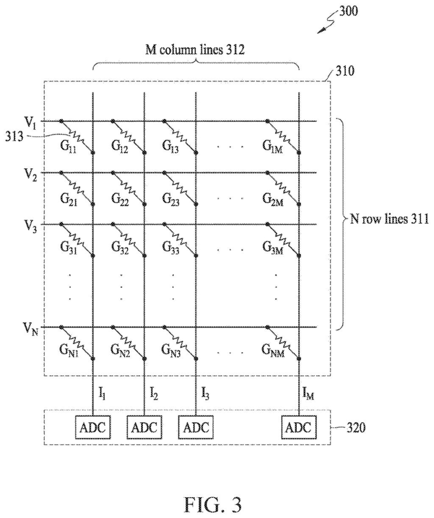
What Samsung's multi-output memory cell chip actually does
A chip inside your phone or laptop is doing millions of math operations just to run an AI feature, like auto-completing a sentence or recognizing a face. Each operation draws power and takes time, and the more steps involved, the slower and hotter the chip gets.
Samsung's patent describes a new way to arrange the memory cells inside an AI chip. Instead of each cell serving only one output, a single memory cell can feed results into multiple output channels at the same time. Think of it like a water main that branches into several pipes instead of running one pipe per house.
The result is that the chip can crunch through AI calculations in fewer clock cycles, meaning less time and potentially less energy per operation. That matters most in phones, earbuds, and wearables where battery life is tight and there's no room for a big cooling fan.
… memory cells disposed at intersecting points between the input lines and the output lines and configured to store weight elements included in multidimensional weight vectors …
Translation: Memory cells sit at grid intersections to store the weights used in artificial intelligence calculations.
How weight data spreads across input and output lines
At the core of most AI chips is an operation called matrix-vector multiplication (multiplying a grid of numbers by a list of numbers, which is how a neural network applies its learned "weights" to incoming data). Traditional chip layouts store each weight value in a memory cell that connects one input line to one output line.
Samsung's design changes that geometry. In this architecture, weight elements belonging to a single multidimensional weight vector (a group of related numbers that together describe one learned connection in the network) are stored across memory cells that all share one input line but connect to two or more output lines. Those output lines all feed into what the patent calls a single "multidimensional output node."
The chip also includes:
- Selectors that route each output line's value to the right adder circuit
- Adders that accumulate results over a set number of clock cycles, building up the final answer incrementally
- A layout where multidimensional input vectors arrive on dedicated input lines that intersect with the output lines at the memory cell positions
By spreading one weight vector's elements across multiple output lines tied to a single input line, the chip avoids redundant read operations and can resolve entire vector calculations in fewer passes, which is the main efficiency claim here.
… selectors configured to transmit a value output from each of the output lines to any one of adders; and the adders configured to accumulate values received from the selectors in a predetermined number of cycles …
Translation: Specialized routing and adding components process the neural network data across multiple timed steps.
What this means for on-device AI processing power
AI workloads are increasingly being pushed off the cloud and onto the device itself, whether that's a phone doing real-time translation or a camera doing object detection without a network connection. The bottleneck in all of those cases is the same: the chip has to do an enormous amount of multiplication and addition, and it has to do it fast enough to feel instant while drawing little enough power to not drain the battery in an hour.
Samsung is one of the world's largest chip designers and manufacturers, so a patent in this area is a direct signal about how the company is thinking about AI silicon efficiency at a hardware level. The specific approach here, reusing a single memory cell position to serve multiple output paths, is the kind of low-level architectural tweak that can compound into real gains when you replicate it across billions of cells on a modern processor. new Big Tech patents in the AI chip space are stacking up quickly, and Samsung's multidimensional vector filing is part of a broader industry push to do more AI math without proportionally bigger or hotter chips.
This is the 44th Samsung filing we've tracked since June in our AI chip wars watchlist, following earlier applications like one on compressing mobile memory and one on smarter memory pre-loading.
The problem this patent targets is real and expensive. Training and running neural networks is essentially a non-stop flood of multiply-and-add operations, and the hardware bottleneck has been a central challenge for every company building AI products. Power consumption and heat are the hard constraints that determine whether an AI feature ships on a phone or gets left in the cloud.
Samsung's approach, threading one weight vector's values through multiple output lines from a single input line, is a legitimate attempt to squeeze more work out of the same physical area of silicon. The adder-and-selector circuit that accumulates results over cycles is a known pattern in analog and mixed-signal AI chip design, so this is refinement work rather than a sharp departure from existing methods.
The honest read is that this is solid engineering on a real problem, but the gains live in the details of implementation. The patent describes the structure clearly, but whether this layout produces meaningful efficiency improvements over competing designs depends on factors like cell density, cycle timing, and manufacturing tolerances that no patent document can fully capture.
Get our take in your Top Stories
Liked this breakdown? Add Patentlyze as a preferred source on Google, and our plain-English take shows up more often in your Top Stories the next time Samsung patent news breaks.
There are more where this came from
We read every patent application Big Tech publishes and send you the ones worth knowing. Plain English, free, every week.
The drawings
19 drawing sheets from US 2026/0252840 A1 · click any drawing to enlarge


Want this weekly breakdown for a company we don't cover? Patentlyze Pro →
Be the first to weigh in