
Sony Patents a Camera That Locks Focus by Measuring Distance and Reading the Scene
Most cameras rely on a single method to lock focus, and that method can fall apart in dim rooms, bright sun, or when a subject moves fast. Sony's new patent describes a processor that cross-checks two separate data streams to keep the focus accurate no matter how the environment changes.
What Sony's dual-source autofocus system actually does
Autofocus fails most often when the scene changes: a cloud passes over, someone walks in front of a light, or your subject steps back into shadow. Today's cameras usually lean on one measurement method, and when that method gets confused, the image goes soft.
Sony's patent describes a system where a depth-sensing chip and a regular camera sensor feed data to a central processor at the same time. That processor figures out the best focus position by weighing both sources together, rather than trusting just one. It can also tell the depth sensor to change how it fires its light pulses, adjusting the timing, brightness, and position of each pulse to get a cleaner reading.
The result is a camera that adapts its focusing strategy on the fly, so you spend less time hunting for the right shot and more time actually taking it.
… an application processor that generates focus control information of the imaging device on a basis of the distance measurement data and the image data.
Translation: The main chip adjusts camera focus by combining distance measurements with visual scene data.
How the processor blends depth data with image frames
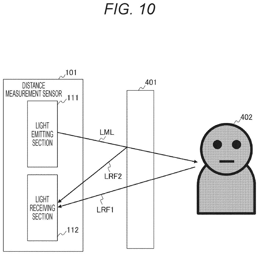
Distance measurement sensors (like the time-of-flight chips found in many modern phones) work by firing pulses of infrared light at a subject and timing how long the light takes to bounce back. That gives the camera a depth reading, but the reading can be thrown off by reflective surfaces, bright ambient light, or objects partially blocking the path.
Sony's patent puts an application processor (the main chip that runs camera logic) in charge of combining that depth data with the actual image data coming off the camera sensor. Instead of the autofocus system treating these as separate inputs, the processor fuses them into a single set of focus control instructions for the lens.
The processor also sends distance measurement control information back to the depth sensor itself, tuning parameters such as:
- Light emission interval (how often pulses fire)
- Light emission intensity (how bright each pulse is)
- Light emission position (where on the scene the sensor aims)
- Continuous light emission count (how many pulses in a burst)
- Light emission pulse width (how long each pulse lasts)
- Light reception position (which part of the sensor receives the return signal)
This feedback loop means the depth sensor is not operating at fixed settings. It adjusts in real time based on what the processor learns from the image, which is the core engineering idea behind the filing.
… output distance measurement control information including at least any one of a light emission interval, a light emission intensity, a light emission position, a continuous light emission count, a light emission pulse width, or a light reception position to the distance measurement sensor.
Translation: The processor can finely tune how the distance sensor flashes light and receives signals.
What this means for cameras in tricky light conditions
Autofocus quality is one of the top reasons people choose one camera or smartphone over another, and improving it through smarter processor logic rather than bigger, heavier lenses is a path Sony has strong incentive to pursue across both its consumer cameras and the image sensors it sells to other manufacturers.
Sony supplies camera sensors to a large share of the smartphone market, so a focusing architecture developed here could eventually influence products well beyond Sony's own lineup. Big Tech patent news in the camera-sensor space has been tracking a broader push by chipmakers to move more imaging intelligence onto dedicated processors, and this filing fits that pattern directly.
This is the 32nd Sony chip patent we've tracked since May, adding to a run that includes one cutting noise in camera chips and one syncing parallel image threads in our chip patent coverage.
The cost of combining a depth sensor and a camera feed into one decision-making loop is timing. In a fast-moving scene, the depth reading and the image can be captured at slightly different moments, and the processor has to treat them as if they agree. That gap is where focus errors sneak in, and it is a real price to pay for a system that promises better accuracy.
Sony appears to be betting that the gain in difficult lighting and complex scenes outweighs that risk, which is a reasonable bet for portraits and slow video but a harder sell for sports photographers.
The quieter opportunity is in the chips Sony sells to phone manufacturers. If this logic ships inside the sensor itself, phone makers get better autofocus without changing any hardware, and Sony shapes how cameras behave across millions of devices without anyone noticing the hand on the lever.
Get our take in your Top Stories
Liked this breakdown? Add Patentlyze as a preferred source on Google, and our plain-English take shows up more often in your Top Stories the next time Sony patent news breaks.
There are more where this came from
We read every patent application Big Tech publishes and send you the ones worth knowing. Plain English, free, every week.
The drawings
23 drawing sheets from US 2026/0255059 A1 · click any drawing to enlarge


Want this weekly breakdown for a company we don't cover? Patentlyze Pro →
Be the first to weigh in