
Sony Patents Camera Chip Technology That Reduces Digital Noise in Photos
Sony is working on a way to clean up noisy image signals right inside the camera sensor chip, before any dedicated image processor even gets involved.
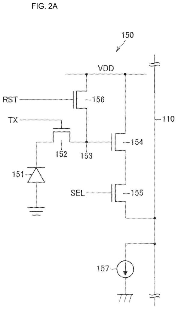
What Sony's in-sensor switching trick actually does
A security camera stares at an empty hallway all night. Every frame it captures carries tiny electrical errors baked into the sensor itself, and those errors degrade every photo or video you ever take.
Sony's patent describes a circuit built directly into the image sensor that can switch between reading real pixel data and reading a clean reference signal. By comparing those two, the chip can identify and subtract its own electrical noise on the fly, without waiting for a separate processor to clean things up later.
The result is that the raw signal coming off the sensor is already in better shape. For everyday cameras from smartphones to security systems, that means less grain in low light and more accurate colors, all handled at the point where the image is first captured.
a first transistor configured to receive the reference signal via a first capacitor; a second transistor configured to receive the first pixel signal via a second capacitor; and a first switch unit coupled to the second capacitor …
Translation: The chip uses dedicated circuits and switches to handle pixel data and reference signals.
How the comparator and capacitors filter out bad readings
The patent describes an imaging device built around a smarter comparator circuit sitting right at the pixel level of the sensor.
Here is how the key pieces fit together:
- A pixel array captures incoming light and outputs raw pixel signals through photoelectric conversion (turning photons into electrical current).
- A reference voltage generation unit produces a clean, known electrical signal with no image data in it.
- A switch unit toggles between feeding the comparator the real pixel signal or the reference signal.
- A pair of capacitors and transistors inside the comparator receive both signals and compare them.
The comparator uses those two inputs to identify the difference between what the pixel actually saw and what the baseline electrical environment looks like. That difference, stripped of baseline noise, is the true image signal.
This approach is called correlated double sampling in chip design: you read the signal twice (once with data, once without) and subtract the noise. What is unusual here is how tightly the switching circuit is integrated into the comparator itself, allowing the first and second voltages to be applied by simply flipping a single switch rather than routing signals through more external circuitry.
… an imaging device including a signal output unit configured to output a predetermined signal and a switch unit configured to output either an output from the signal output unit or an output from a pixel array …
Translation: The camera alternates between processing actual image pixels and reference signals to clean up the picture.
What this means for camera quality at the chip level
For anyone using a camera in low light, whether that is a phone at a dinner table or a security sensor in a dim parking lot, sensor-level noise is the enemy. Fixing it in software or in a downstream processor works, but it takes time and processing power, and some damage is already done by the time raw data leaves the sensor. Cleaning the signal at the point of capture is a more efficient approach.
Sony Semiconductor Solutions supplies image sensors to a huge range of device makers, so improvements at this level can ripple through many products at once. Chip-level patents like this one sit alongside a steady flow of new Big Tech patents in imaging and semiconductor design, reflecting how much competition there is to squeeze better performance out of smaller, more power-constrained sensors.
Sony's 354th filing we've tracked in our Sony coverage since May joins earlier work on copying a director's camera style and smarter pixel reading.
For anyone taking photos, the real benefit is simple: sharper, cleaner pictures in dim rooms where photos usually come out grainy.
The underlying trick has existed in camera sensors for decades. Fitting it into a smaller, lower-power package matters most for tiny cameras where every extra component costs money.
You would never see this part or know it exists. But you would notice it was missing the next time a photo taken in a dark room came out looking like a blizzard of static.
There are more where this came from
We read every patent application Big Tech publishes and send you the ones worth knowing. Plain English, free, every week.
The drawings
24 drawing sheets from US 2026/0246478 A1 · click any drawing to enlarge


Want this weekly breakdown for a company we don't cover? Patentlyze Pro →
Be the first to weigh in