
Apple Patents a Tiny Light Projector That Maps Surfaces With Precise Dot Patterns
Apple has filed a patent for a new kind of light projector that uses ultra-thin optical surfaces, engineered at the nanometer scale, to flood a scene with thousands of precisely aimed dots of infrared light. It's the core ingredient of any system that needs to measure depth and build a 3D map of whatever is in front of a camera.
What Apple's dot-pattern depth sensor actually does
You're holding your phone up to unlock it, and in a fraction of a second it figures out the exact shape of your face in three dimensions. That trick relies on a tiny projector that splashes a grid of invisible infrared dots across your features, then reads how they distort to calculate depth. Apple's new patent describes a much more compact, precise way to build that projector.
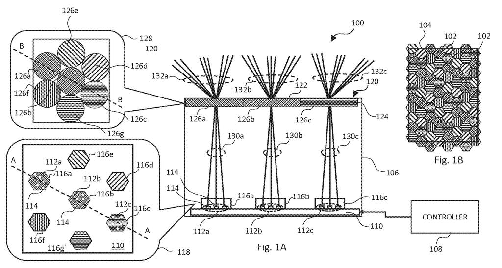
Instead of a stack of separate lenses and beam-splitters, the design uses a single ultra-thin layer of nano-scale optical structures, called a metasurface, placed directly over the light-emitting chip. Each microscopic window in that layer grabs the light from a cluster of emitters below it, focuses it, and fans it out at multiple precise angles simultaneously. The result is a dense, repeating grid of dots covering the entire target area.
The big deal is that doing all of that in one flat layer, bonded directly to the emitter chip, means the projector can be smaller and potentially more accurate than today's multi-component designs. Smaller projectors open space for thinner devices or more powerful sensing in the same footprint.
… each aperture configured to receive, collimate and split the beams emitted by a respective array of the emitters into a respective group of collimated sub-beams, so as to direct the collimated sub-beams toward a target at different, respective angles to form a pattern of spots on the target …
Translation: Each opening catches laser light and splits it into an angled grid of beams.
How the metasurface splits and aims each beam
The patent describes what Apple calls an optoelectronic apparatus, meaning a device that converts electrical signals into precisely directed light. The hardware has three main layers stacked on top of each other.
- Semiconductor substrate with emitter arrays: The bottom layer is a chip carrying multiple groups of tiny light sources, likely VCSELs (vertical-cavity surface-emitting lasers, the same type used in Face ID today). Each group of emitters acts as one unit.
- Optical substrate: A thin transparent layer mounted directly above the emitter chip, providing a stable base for the optical layer on top.
- Optical metasurface: The key innovation. This is a flat surface covered with precisely shaped nano-scale features, patterned into multiple apertures (openings), one aligned above each group of emitters below. Each aperture simultaneously collimates the light (focuses it into parallel beams, like a lens), and splits it into several sub-beams aimed at different angles.
The combined effect is that the projected pattern on a target, such as a face or a room, is a tiled mosaic of dots: multiple copies of the emitter array's layout, spread across the full field of view. A depth camera then photographs those dots and, because their positions shift predictably when they hit a curved or uneven surface, software can reconstruct precise 3D geometry.
The entire optical job, collimation plus beam-splitting plus angle control, happens in a single flat layer rather than across a series of separate optical components.
An optoelectronic apparatus includes a semiconductor substrate and multiple arrays of emitters disposed on the semiconductor substrate and configured to emit beams of optical radiation.
Translation: The device uses a silicon chip fitted with multiple rows of tiny light emitters.
What this means for Face ID and spatial sensing
Depth sensing, the technology that makes Face ID work and lets AR headsets understand physical space, depends on projecting a stable, dense pattern of light onto a scene. The precision of that pattern sets a ceiling on how accurately the system can measure shape and distance. A projector that can do more with less hardware, fewer separate lenses, smaller total thickness, is directly valuable for any device where space is tight.
Apple's interest in compact depth-sensing hardware shows up consistently across its device lineup, from iPhone front cameras to the Vision Pro's spatial mapping. A flatter, more integrated projector could improve Face ID reliability in lower-power modes, shrink the sensor notch further, or scale to new form factors like glasses where every millimeter of thickness matters to you as a wearer.
Apple's 69th filing Apple AR glasses we've tracked since May follows the strap-held processor and the lens frame design with yet another step toward wearable displays.
Every face-unlock that fails in dim light, every AR headset that misreads where your hand is, traces back to the same root cause: bending light precisely into hundreds of tiny dots requires a stack of carefully aligned lenses inside a space that keeps shrinking as devices get thinner. When that alignment drifts even slightly, the whole sensing system degrades, and the only fix has been more precise manufacturing at higher cost.
Apple's patent attacks that problem by replacing the lens stack with a single flat layer etched to focus and redirect light in one step. The accuracy problem it addresses is not marginal, it is the main reason depth-sensing features are expensive to build reliably at scale.
Whether a flat optical layer can hold its precision across millions of devices in real conditions is a genuine open question, but the problem Apple is aiming at is large enough that even a partial solution would matter.
There are more where this came from
We read every patent application Big Tech publishes and send you the ones worth knowing. Plain English, free, every week.
The drawings
9 drawing sheets from US 2026/0287835 A1 · click any drawing to enlarge


Want this weekly breakdown for a company we don't cover? Patentlyze Pro →
Be the first to weigh in