
AMD Files Patent for a Single Chip That Merges AI Processing With Graphics
AMD's chip design arm Xilinx has filed a patent for a single integrated circuit that wires an AI processing array directly to graphics processing cores, letting both sides share the same memory without the delays that come from shipping data between separate chips.
What AMD's fused AI-and-graphics chip actually does
You're running an AI model and a graphics renderer at the same time, and your computer keeps shuffling data back and forth between two separate chips. That handoff is slow, and the gap adds up fast.
AMD's patent describes a chip design where the AI side and the GPU side live together on one piece of silicon. The AI processing blocks and the graphics cores can both reach into a shared pool of local memory, coordinated by circuitry that keeps them from stepping on each other's data. Think of it like two workers sharing one filing cabinet, with a clear system for who opens which drawer and when.
The key detail is the shared memory setup. Instead of the AI and graphics sections sending messages to each other across a slow external bus, they read and write the same storage directly. That's the design bet AMD is making here.
a data processing array comprising data processing elements (DPEs) and a network of links and configurable switches; and a first compute unit configured to interface with a first subset of the DPEs via the network of links and switches …
Translation: The chip uses a network of switches to connect computing units directly with data processing elements.
How the AI array and GPU cores share the same memory pool
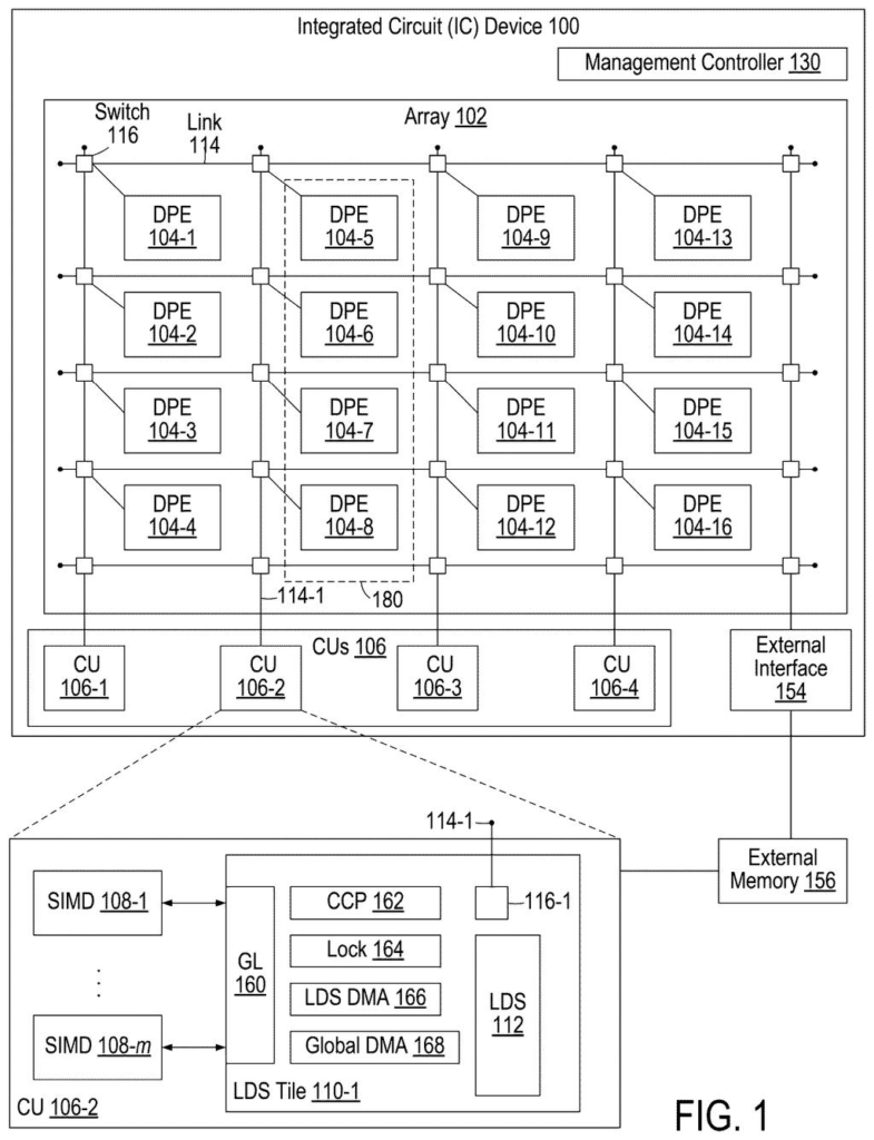
The patent describes an integrated circuit (IC) that combines two kinds of processing hardware that are usually kept separate: an AI engine (a grid of programmable data processing elements, or DPEs) and a graphics processing unit (GPU).
The GPU side is organized into shader engines, each containing multiple compute units (CUs). Each compute unit holds a set of SIMD processors (single-instruction multiple-data processors, meaning they run the same operation on many data points at once, which is how GPUs crunch through graphics and math), plus a local data storage system (LDS), which is a small, fast patch of on-chip memory.
The novel part is the synchronizer circuitry inside each compute unit. It acts as a traffic controller, deciding when the SIMD processors can read or write the LDS and when the AI processing elements can do the same. Both sides connect through a network of links and configurable switches that runs across the chip, letting any compute unit talk to any subset of DPEs.
- Each compute unit is paired with a specific group of AI processing elements.
- Multiple compute units share a shader engine.
- Multiple shader engines can exist on the same chip, all linked through the same network.
The design allows the AI array and the GPU cores to pass data through shared memory rather than across external connections, cutting the round-trip time significantly.
An integrated circuit (IC) device having an integrated artificial-intelligence engine (AIE) and a graphics processing unit (GPU) …
Translation: A single silicon chip combines a graphics processor with artificial intelligence hardware.
What a fused AI-GPU chip could mean for your devices
Chips that handle AI and graphics separately must move data between them constantly, and that movement costs time and power. Fusing both onto one die with shared memory is a way to cut that cost at the hardware level, which matters for anything from gaming to real-time AI image generation to robotics.
For you as a consumer, the practical upside would be devices that run AI and graphics together more efficiently, potentially with less heat and better battery life. This is still a circuit architecture described in a patent, so there is a real gap between this filing and a shipping product. But AMD's interest in tightly coupled AI and compute silicon suggests the company is working toward chips where the AI layer is a first-class citizen alongside graphics, not an afterthought bolted on.
AMD's 41st filing we've tracked since May in the AI chip race follows earlier work on a header that cuts wasted data and shared memory between processor groups.
Getting this design into a real product requires building new physical hardware, not writing new software. That means years of chip design, testing, and manufacturing before anything ships.
The architecture described here has real roots in chips AMD already makes, which suggests this is an engineering proposal with legs rather than a speculative sketch. The core idea is letting the AI processing parts and the graphics parts share a small, fast memory pool in a coordinated way, and that coordination mechanism is the novel piece AMD is protecting.
The shortest path to a product would likely involve AMD's existing graphics chip roadmap absorbing ideas from its AI accelerator work, but nothing in this document reveals a timeline or a named product.
There are more where this came from
We read every patent application Big Tech publishes and send you the ones worth knowing. Plain English, free, every week.
The drawings
10 drawing sheets from US 2026/0301107 A1 · click any drawing to enlarge


Want this weekly breakdown for a company we don't cover? Patentlyze Pro →
Be the first to weigh in