
AMD Patents a Shared Memory Block That Sits Between AI Processor Groups
Moving data around inside a chip is one of the biggest drags on AI performance. AMD has filed a patent describing a memory tile that sits between two clusters of AI processors, letting both sides share the same data storage directly.
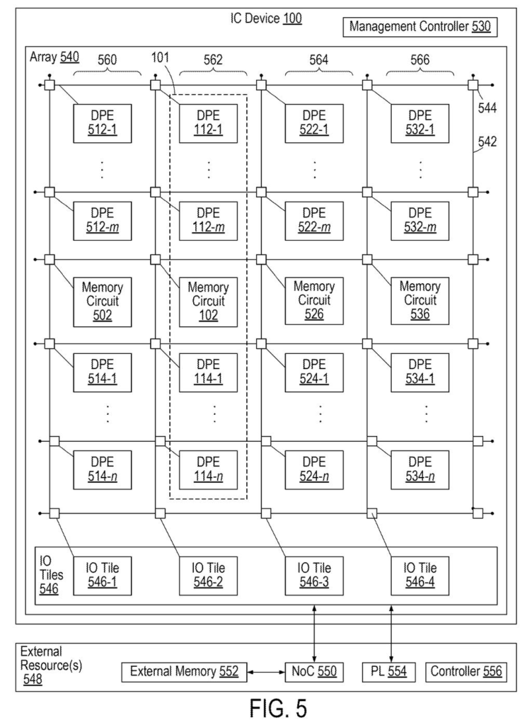
What AMD's shared-memory chip layout actually does
Ever wondered why a faster AI chip doesn't always mean faster AI results? A lot of the time, the bottleneck isn't the processors doing the math, it's how quickly they can get data in and out.
This patent describes a chip design where a block of memory sits in the middle, with AI processing units on either side. Each side has its own door into that shared memory, and a small coordination circuit makes sure both sides don't try to read or write at exactly the same time and cause a conflict. Think of it like a shared office filing cabinet with two sets of drawers, one facing each team, and a manager making sure nobody opens the same drawer simultaneously.
The goal is to reduce the distance data has to travel on the chip, which saves time and power. Instead of AI processors waiting in line for a distant memory bank, they each have a nearby, direct connection to the same pool of data.
a memory circuit comprising: a memory bank; a first input/output (IO) interface along a first edge of the memory circuit, configured to permit access to the memory bank; a second IO interface along a second edge of the memory circuit …
Translation: The memory chip has two separate connection points on different sides to let different processors reach the same data.
How the memory tile coordinates two processor clusters
The patent describes an integrated circuit (IC) device, meaning a single chip, built around a memory circuit that has two separate input/output (IO) interfaces. Each interface sits on a different edge of the memory block, either opposite sides or adjacent sides.
On one side of the memory block sits a first set of data processing elements (DPEs), which can include AI engines (AIEs). A second set of DPEs sits on the other side. Each set connects to the shared memory bank through its own dedicated interface, so both groups of processors can access the same data without being routed through a longer, slower path.
The key ingredient is the synchronization circuitry: logic that manages who gets to access the memory bank, and when, across both interfaces. This prevents read/write collisions (two processors trying to modify the same data at the same moment) without requiring the processors to coordinate with each other directly.
The design fits within Xilinx's existing AI Engine (AIE) tile architecture, where chips are assembled from repeating functional blocks. Inserting a dedicated memory tile between AIE tiles is meant to shorten the data path and reduce the overhead of moving data across the chip.
The IC device may further include a first set of data processing elements (DPEs) that access the memory bank via the first IO interface, and a second set of DPEs that access the memory bank via the second IO interface. One or more of the DPEs may include an artificial intelligence engine (AIE).
Translation: Two distinct groups of AI processors share the same memory block by plugging into opposite sides of it.
What this means for AI chip design and data bottlenecks
For AI workloads, memory access speed often determines overall performance more than raw compute power. Chips that do matrix math quickly but wait long periods for data end up underutilizing their processors. A shared memory tile placed physically between two processor clusters cuts down that waiting time by keeping data close to where it's needed.
AMD's string of AI chip architecture filings reflects how seriously the industry is rethinking chip layout for AI workloads. If this memory tile design makes it into a future product, it could improve performance per watt on tasks like AI inference, the process of running a trained model to generate answers, without requiring a fundamentally new manufacturing process.
AMD's 39th filing we've tracked since May in our AI chip wars watchlist follows their work on neighbor memory sharing and self-scheduling GPU math, showing a pattern of chips doing more work on their own.
Getting this from a patent filing to a product customers can buy requires new physical hardware, not a software update. The design describes a specific arrangement of memory and processing blocks etched into silicon, which means AMD has to fabricate it, test it, and validate it before anything ships.
The core idea is a shared memory block that sits between clusters of AI processors and lets both sides read and write in an orderly way. Keeping processors fed with data fast enough is one of the central problems in AI chip design, and the coordination circuitry described here addresses that directly.
Nothing in this document shows the design has been tested in actual silicon, so the shortest path to a product still runs through years of engineering work that goes unmentioned here. If that coordination holds up at speed and volume, this layout could matter to customers who buy AMD's AI hardware down the road.
There are more where this came from
We read every patent application Big Tech publishes and send you the ones worth knowing. Plain English, free, every week.
The drawings
10 drawing sheets from US 2026/0288334 A1 · click any drawing to enlarge


Want this weekly breakdown for a company we don't cover? Patentlyze Pro →
Be the first to weigh in