
Apple Files Patent to Erase Faint Brightness Bands Around Screen Cutouts
Cut a hole in a screen and the wires around it behave differently, which can leave faint bands of uneven brightness. Apple's filing fixes the shading by editing the picture itself, pixel by pixel.
What Apple's screen-cutout shading fix does
A phone screen has a small hole cut into it so a sensor can see out. The thin wires that carry picture signals to each pixel have to detour around that hole. You never see the wires, but the detour changes how electricity moves through them, and the picture nearby can come out slightly brighter or darker, in faint bands.
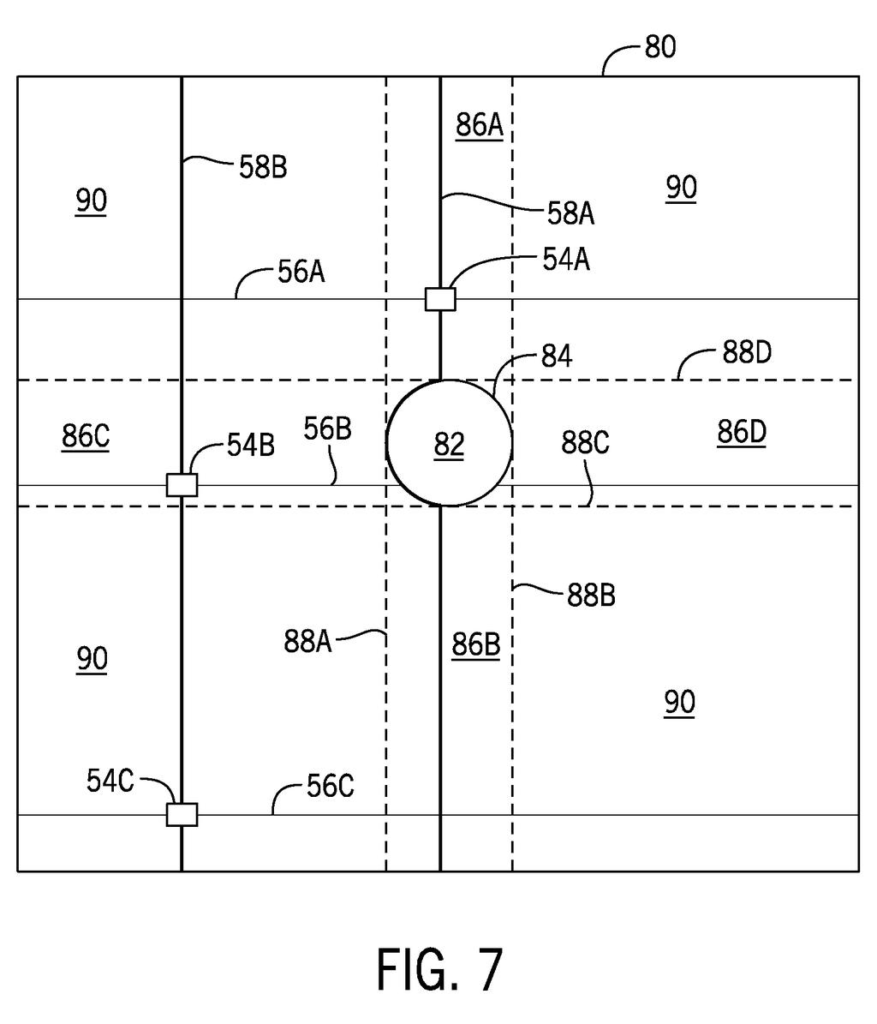
Apple's filing describes a fix made in the picture data. Instead of rebuilding the panel, the display edits the image before it reaches the pixels near the hole. It marks off zones above, below, left and right of the hole, and each zone gets its own small correction.
The correction also shifts with conditions, such as the screen's temperature and whether it is refreshing 60 or 120 times per second. Pixels far from the hole are left alone. The goal is a screen where the shading around the hole gives it away less.
… apply a banding artifact compensation to adjust image data for a pixel based on the pixel being disposed in a logical zone adjacent to an impedance distorting region …
Translation: The system tweaks pixel brightness near cutouts to fix weird visual banding issues.
How Apple splits the area around a hole into zones
The filing centers on what it calls an impedance distorting region (IDR), meaning any part of a display that disturbs the electrical behavior of the panel. The main example is a hole or notch cut for a sensor. Other examples are patches with a different pixel density and spots where wires bend.
When a signal wire curves around a hole, its resistance and capacitance (how much it resists current and how much charge it stores) change. Pixels on that wire get a slightly shorter window to load their picture data, so brightness or color drifts. That drift shows up as banding.
The fix works in four steps:
- Define logical zones (top, bottom, left and right of each hole) using row and column numbers, which is a cheap check to run.
- Produce zone data by interpolating (filling in values between known points) across the columns of a zone.
- Scale the result using temperature, refresh rate, dimming level or voltage. In the filing's example, 120 Hz can use a value double or half the 60 Hz one.
- Adjust the pixel's image data and send it on. Several holes mean several correction circuits that switch on or off per pixel, and overlapping zones stack their corrections.
The corrections can be calibrated at the factory by photographing test images and storing the results in a lookup table. The filing also describes changing the drive voltage on lines with different resistance, either instead of or alongside the picture edit.
Image data transmitted to pixel via lines that route around or through the IDR may be adjusted to compensate for parasitics that may be introduced by the IDR or routing around or through the IDR.
Translation: Signals routed around physical cutouts get corrected for electrical interference.
What this means for phones with screen cutouts
If phone, tablet or watch makers keep cutting holes in screens for sensors, every one of those holes risks a visible shading problem. This approach would let a screen hide that flaw using a correction applied to the picture, so the hole is harder to spot when you look at a plain white or gray background.
The filing also says the method takes up less silicon than adding dummy circuitry to balance out the wires, and that skipping pixels far from the hole saves power. For you, that could mean a cleaner-looking display without a trade in battery or panel space. The filing lists iPhone, iPad, MacBook and Apple Watch as example devices.
Apple's 42nd filing in the Display patents we cover since May follows a tilt and hand control idea and a sharpest-frame grabbing system.
Fixing a screen flaw by editing the picture means the fix lives in numbers, and numbers can be wrong. The filing says the corrections come from a factory step: show test images, photograph the screen, and record where the color or brightness drifts. That adds work to every panel made, and the filing does not say what happens if the screen's behavior shifts as it ages.
The alternative is extra dummy circuitry that balances out the wires around the hole. The filing says its approach uses less silicon and a smaller footprint than that. It also skips pixels far from the hole, which saves power.
Smaller, cheaper and lower power in exchange for a bit of factory calibration reads as a good trade. It is routine display engineering, and it only matters if phones keep cutting holes in the screen.
Get our take in your Top Stories
Liked this breakdown? Add Patentlyze as a preferred source on Google, and our plain-English take shows up more often in your Top Stories the next time Apple patent news breaks.
There are more where this came from
We read every patent application Big Tech publishes and send you the ones worth knowing. Plain English, free, every week.
The drawings
10 drawing sheets from US 2026/0331022 A1 · click any drawing to enlarge


Show the other 2 sheets


Want this weekly breakdown for a company we don't cover? Patentlyze Pro →
Be the first to weigh in