
Samsung Files Patent for Memory Chips That Do Some of an AI's Math Themselves
Your AI chatbot spends a lot of its time waiting for data to arrive from memory. Samsung's filing puts calculators inside and beside the memory so the lightest steps never have to travel.
What Samsung's three-tier memory chip actually does
Ever watched a cook sprint to the pantry for every ingredient, carry it back to the stove, then repeat? That back-and-forth wastes more time than the cooking itself. Computers running AI chatbots have the same problem: the chip doing the math spends a lot of its time waiting for data to arrive from memory.
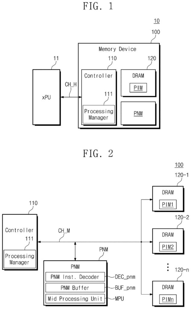
Samsung's filing tries to fix that by letting the memory do some of the work. It describes a memory device with three places where math can happen: the main processor (the chip that usually runs AI), a helper unit sitting next to the memory, and tiny calculators built right inside the memory chips. Each step of an AI model goes to whichever place fits it best.
The most math-heavy steps stay with the main processor. Medium steps go to the helper unit. The light steps that mostly just read lots of data are handled inside the memory itself, so that data never has to travel at all.
A heterogeneous computing memory device comprising: a memory including a processing-in-memory (PIM) unit; a processing-near-memory (PNM) unit; and a controller configured to receive first to third requests from an external processing device …
Translation: The chip combines standard storage with built-in processors to handle tasks right where the data lives.
How each AI layer gets routed to its best worker
The core is a memory device with a controller (the traffic manager) that takes requests from an outside processor over a host channel (the link to the main chip). Each request names one layer of an AI model, and each layer has a computational intensity: how many math operations it needs per byte of data it reads.
- Highest intensity: the controller reads the stored data and sends it out to the main processor, which does the math.
- Middle intensity: the controller tells a processing-near-memory unit (a helper chip beside the memory) to pull data over the memory channel and process it.
- Lowest intensity: the memory does the work itself using processing-in-memory circuits (small calculators built into the memory chips), so the data never leaves.
The description walks through chatbot-style language models. One common form of the attention step (multi-head attention) is low intensity and runs inside the memory. Two other forms (grouped-query attention and mixture-of-experts feed-forward layers) land in the middle tier. Claim 9 covers that split.
The filing also describes extras: the main processor can work on one piece while memory finishes another, the link can use the CXL standard (a fast connection for pools of memory), and the parts can be stacked in one package.
… controls the PNM unit to process the second layer in response to the second request, and controls the memory to process the third layer in response to the third request.
Translation: The system routes different parts of an AI workload to different processing units based on how complex the math is.
Why AI memory bottlenecks matter for data centers
If this works, you would feel it indirectly: AI chatbots that answer faster and cost less to run in data centers. A big limit on chatbot speed is how quickly data moves from memory to the processor, and the processor often sits idle waiting. Doing the lightest steps inside the memory cuts that traffic, and the middle steps get their own helper instead of crowding the main chip.
Samsung makes memory, so a design that makes memory do more of the work fits naturally with what it sells. The filing covers several physical forms, from memory modules to stacked chips in one package to data-center servers, so it is meant to fit many setups. It gives no speed or energy numbers, so the size of the gain stays unknown.
Samsung's 62nd filing we've tracked since June in our AI chip competition work, it builds on one keeping chatbots quick and one cutting chip idle time.
Claim 1 covers a memory device that bundles three things at once: calculators inside the memory, a helper unit beside it, and a controller that sends heavy, medium and light layers of work to the right place. Leave out any one of those and the claim no longer fits, so a design with only two tiers falls outside it.
The wording is wide in other ways. Claim 1 says 'layer' and never names a chatbot, and it sets no number for what counts as heavy, medium or light. Only claim 9 narrows things down to language models.
If granted, it would cover any memory device that divides AI work this three-way. The filing gives no speed or energy figures, so the payoff is unproven. The split itself is simple to picture and would be easy to spot in a finished product.
Get our take in your Top Stories
Liked this breakdown? Add Patentlyze as a preferred source on Google, and our plain-English take shows up more often in your Top Stories the next time Samsung patent news breaks.
There are more where this came from
We read every patent application Big Tech publishes and send you the ones worth knowing. Plain English, free, every week.
The drawings
23 drawing sheets from US 2026/0330207 A1 · click any drawing to enlarge


Show the other 15 sheets


Want this weekly breakdown for a company we don't cover? Patentlyze Pro →
Be the first to weigh in