
IBM Patents a Dimpled Chip Surface That Helps Sensors Spot Proteins in Blood
Blood is salty, and that salt can hide the very proteins a sensor is trying to find. IBM's patent application tries to get around it by covering a chip's sensing surface with pits only a few dozen nanometers wide.
What IBM's pitted sensor surface actually does
You're waiting on a lab result, and somewhere a tiny electronic sensor is trying to spot one specific protein in a drop of your blood. That is harder than it sounds. Blood is salty, and the salt surrounds the sensor with a fog of charged particles that muffles the faint electrical signal a protein gives off.
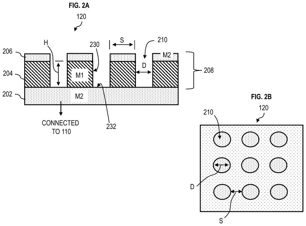
IBM's patent application goes after the problem with the shape of the sensor's surface. Instead of a flat plate, the surface is dotted with tiny pits (or narrow trenches) sitting between low raised walls, all measured in billionths of a meter. Proteins attach to those walls, so the fog muffles the signal less.
In IBM's own estimate for one layout, sensitivity came out about 11 times higher than a flat surface. That is a calculation in the filing, not a lab-proven result.
… a sensing structure coupled to the transducer and configured to receive an analyte, wherein the sensing structure comprises concave portions adjacent to raised portions …
Translation: The sensor uses a specially shaped surface with dips and bumps to catch target molecules in fluid.
How the tiny pits get around salty blood
A biosensor pairs a transducer (the part that turns a chemical event into an electrical signal; in IBM's drawings it is a transistor) with a sensing structure that touches the liquid being tested. Claim 1 covers a sensing structure with concave portions (pits or trenches) sitting next to raised portions. The pits are 10 to 200 nanometers wide and 10 to 200 nanometers apart, and the raised parts stand 5 to 50 nanometers tall.
The description explains the numbers. In blood, salt hides a protein's electric charge once it sits more than about 10 angstroms (roughly 1 nanometer) from the surface, a distance called the Debye length. That limits how well these sensors can detect large proteins. IBM gives 200 nanometers as the upper limit for pit width. It sets 10 nanometers as the lower limit because most proteins would not fit into smaller pits. A typical antibody is about 10 nanometers.
The filing shows several layouts:
- Round pits between pillars, with walls made of a metal such as ruthenium oxide that probe molecules stick to, while the flat areas stay inactive.
- Fin arrays with ultra-shallow trenches only 2 to 5 nanometers tall, which is the focus of the second independent claim.
- Single-metal versions, plus one fabrication method that etches dents through the grain structure of a titanium nitride film.
… where a width of the concave portions ranges from 10-200 nanometers (nm), where a spacing between the concave portions ranges from 10-200 nm, and where a height of the raised portions ranges from 5-50 nm.
Translation: The dimples and bumps are built to extremely precise nanoscale dimensions to trap proteins.
What this means for protein and blood testing
Sensors that read proteins directly in salty fluids like blood are held back by the salt around them. IBM's pitted surface aims to loosen that limit. For one shallow-trench layout, the filing says the geometry allows detection at sub-attomolar levels (extremely tiny concentrations) in physiological buffers (fluids that mimic body chemistry). Those are descriptions and estimates in an application, not lab results you can count on.
The practical angle is manufacturing. The filing says standard semiconductor fabrication techniques (layering, patterning and etching) can build both the transistor and the pitted surface. It names no product and no use beyond testing liquids, so where this lands, if anywhere, is open.
IBM's third filing we've tracked since August in our wearables that read your body watchlist follows their one matching pain to sleep patterns and one linking brain signals to search.
Claim 1 is short, and its breadth is its main feature. It names a transducer, a sensing surface with pits next to raised areas, and three size windows: pits 10 to 200 nanometers wide, 10 to 200 nanometers apart, with raised parts 5 to 50 nanometers tall.
It says nothing about which metal to use, which protein to hunt, or what kind of transistor sits underneath, so many designs could land inside those numbers. The windows themselves are firm limits. A sensor with pits wider than 200 nanometers, or raised parts taller than 50, would sit outside claim 1, and the second independent claim squeezes the raised height down to 2 to 5 nanometers.
If granted, it would fence off a specific geometry for pitted sensor surfaces. Whether that matters depends on whether the filing's sensitivity estimates survive real lab testing, and the text offers calculated estimates only.
Get our take in your Top Stories
Liked this breakdown? Add Patentlyze as a preferred source on Google, and our plain-English take shows up more often in your Top Stories the next time IBM patent news breaks.
There are more where this came from
We read every patent application Big Tech publishes and send you the ones worth knowing. Plain English, free, every week.
The drawings
10 drawing sheets from US 2026/0348900 A1 · click any drawing to enlarge


Show the other 2 sheets


Want this weekly breakdown for a company we don't cover? Patentlyze Pro →
Be the first to weigh in