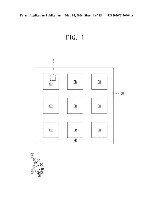
Samsung Patents a New Contact Pad Layout for 3D Memory Wordlines
As 3D NAND flash stacks more and more memory layers on top of each other, the tiny metal contact pads that connect…
Every Big Tech patent in the hardware category, in plain English. Updated weekly from USPTO.
As 3D NAND flash stacks more and more memory layers on top of each other, the tiny metal contact pads that connect…
Deep inside a chip factory, the difference between a working transistor and a dead one can come down to a single masking…
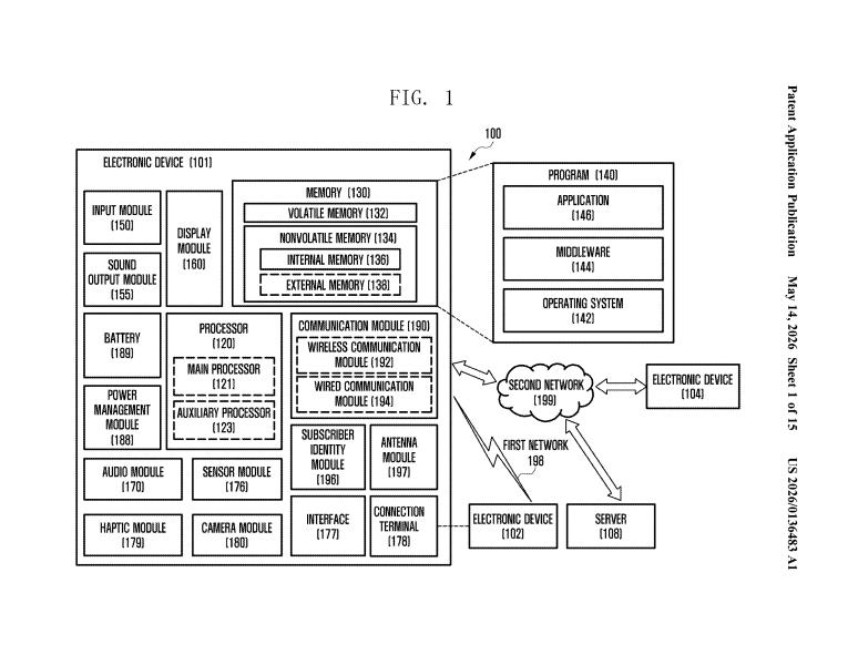
Imagine your smartwatch notices you've sat down at your desk and automatically tells your PC to pick up where your phone left…
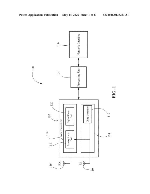
Radar chips are only as accurate as their analog circuitry — and that circuitry is never perfect. Samsung's new patent describes a…
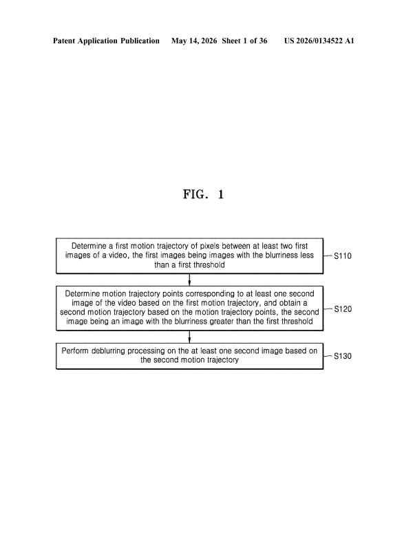
Every video has a few frames ruined by motion blur — a fast pan, a sudden gesture, a poorly timed shutter. Samsung's…
Getting two separate circuit boards to talk to each other across a mechanical hinge — without adding bulk or breaking when the…
Tiny LEDs lose a surprising amount of light through their exposed edges — Samsung's new patent wraps each one in an ultra-thin…
Samsung is refining how air moves inside its clothing care cabinets — and the key insight is that not all the air…
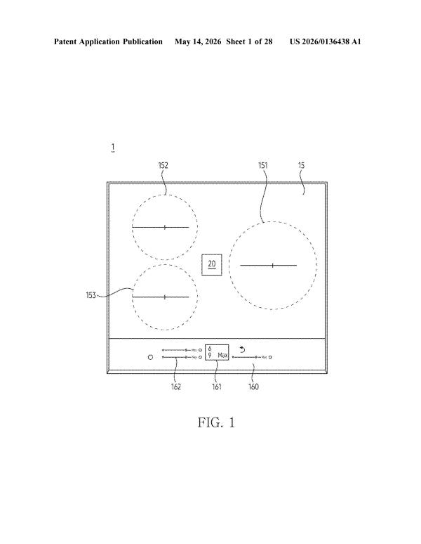
Samsung is patenting a way for induction cooktops to automatically detect when something on the burner reaches a boil — no thermometer,…
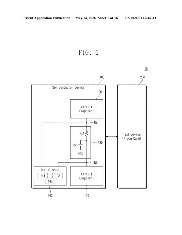
As chips get smaller and the wires connecting their components shrink to nanometer scales, verifying those connections without destroying the chip becomes…
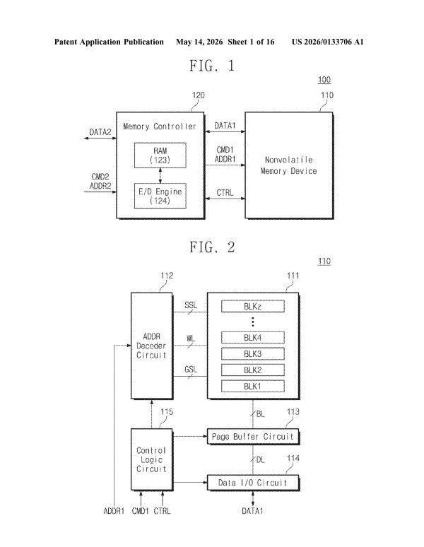
Flash memory wears out partly because not all bit patterns are equally kind to the cells that store them. Samsung's new patent…
Samsung Display is rethinking what happens inside the light-emitting heart of an LED. By splitting the active layer into two chemically distinct…
One Big Tech patent every Sunday. Free.