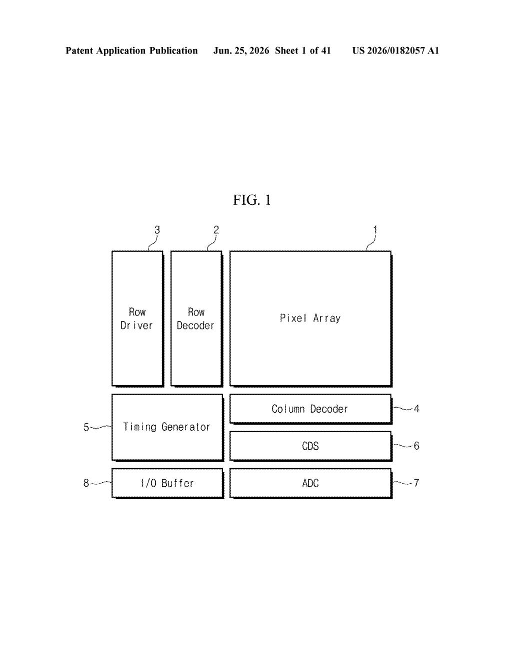
Samsung Patents an Image Sensor That Traps Air Between Its Color Filters
Samsung is filing patents on a camera sensor that deliberately leaves tiny air pockets sealed inside its structure, and the reason comes down to basic physics: air bends light differently than glass or plastic.
What Samsung's air-gap image sensor actually does
Picture a camera sensor as a tiny layered sandwich. Light comes in, passes through a grid of colored filters (one per pixel, each tuned to red, green, or blue), and lands on the actual light-catching layer below. In most sensors today, every gap between those filters is filled with some kind of solid or liquid material.
Samsung's patent describes a design where those gaps are left as sealed air pockets instead. A thin glass plate sits on top and closes off the air space, keeping it stable inside the sensor.
Why bother? Air has a much lower refractive index than solid materials, meaning light crosses the boundary between filter and air at a sharper angle. That helps keep each pixel's light more contained, reducing the chance that a photon meant for one pixel bleeds over into a neighbor. Less crosstalk between pixels generally means sharper, cleaner images.
How the air gaps sit inside the sensor stack
The sensor is built in layers stacked on a silicon substrate. From the bottom up, the key layers are:
- A transmissive insulating layer on the back surface of the substrate (letting light through while blocking electrical interference)
- A grid of color filters, one per pixel
- Planarization patterns sitting on top of the filters (flat-topped structures that level off the uneven filter surface)
- A first air gap formed inside the recesses between those filter-and-pattern stacks
- A glass substrate that caps the top, sealing the air gap closed
The air gap is not accidental empty space. It is a deliberate, enclosed cavity. The glass lid prevents contamination or collapse while maintaining the low-density air interface.
The claim is tightly focused on the geometry: air trapped between the color filters and between the planarization patterns, with the glass closing the top. This is a structural patent about sensor architecture, not about signal processing or software correction.
What this means for Samsung camera hardware
Image sensor crosstalk (where light leaks from one pixel into an adjacent one) gets worse as pixels shrink. As Samsung and its competitors push toward higher megapixel counts in smaller sensor areas, each individual pixel gets tinier and the walls between them matter more. An air interface is one of the most effective passive barriers available because of its optical properties.
If this architecture makes it into production sensors, you would likely see the benefit in low-light or high-detail shots, where color accuracy and edge sharpness are most sensitive to crosstalk. Samsung supplies image sensors not just for its own Galaxy phones but for many other device makers, so the potential reach of a structural improvement like this is wide.
Get one Big Tech patent every Sunday
Plain English, intelligent commentary, no hype. Free.
Editorial commentary on a publicly published patent application. Not legal advice.