
Samsung
Samsung · Antenna & radio · Filed Dec 30, 2025 · USPTO published Jun 25, 2026 · Jun 25 release
Samsung Patents Signal-Sending Pads Built Into a Device's Internal Frame
Samsung wants to turn a device's internal skeleton into part of its antenna system, hiding signal-sending patches inside the structural frame rather than dedicating separate space to them.
- Publication number
- US 2026/0180203 A1(US20260180203A1)
- Applicant
- SAMSUNG ELECTRONICS CO., LTD.
- Filed · Published
- Dec 30, 2025 · Jun 25, 2026
- Inventors
- Sumin YUN, Hosaeng KIM, Seongjin PARK, Hyungjoo LEE
- Status when we published
- Waiting for an examiner
- Document
- 17 claims
- US classification
- 343/702
- Parent application
- Continuation of PCT/KR2024/009132 (filed Jun 28, 2024)(PCTKR2024009132)
What Samsung's frame-embedded antenna actually does
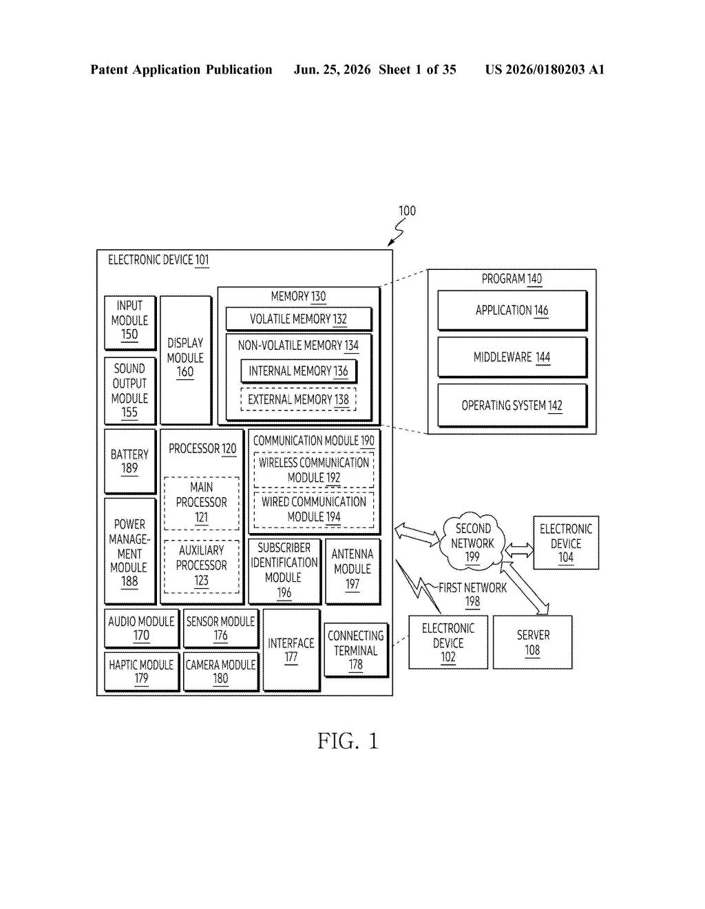
Imagine the rigid internal frame that holds your phone or tablet together. Right now that frame is mostly just structural, keeping the screen and back panel from flexing. Samsung's patent proposes putting small antenna patches directly on the side of that frame, so it does double duty: holding the device together and sending and receiving wireless signals.
The patches are designed to work with a specific type of signal called circular polarization, which spins as it travels through the air. That spin makes the signal more reliable when you tilt or rotate your device, since the antenna can pick it up from multiple angles instead of needing to be perfectly aligned.
The frame connects to the main circuit board and to a metal layer on either the top or bottom face of the device, which helps the whole setup function as a proper antenna system. The idea is to free up internal space that would otherwise be taken up by a standalone antenna component.
How the conductive patches sit inside the support structure
The patent describes a device built around a support member (essentially an internal structural bracket) that has three sections: a top face, a bottom face, and a side wall running between them. The side wall is where the action happens.
A set of conductive patches (small, flat metal elements) are placed on the surface of that side wall. Each patch is wired to the device's wireless communication circuit on the main PCB. Together, the patches form an antenna array that handles wireless transmit and receive functions.
The key design choice is circular polarization (a signal whose electromagnetic field rotates in a corkscrew pattern as it travels). Compared to linear polarization, circular polarization is less sensitive to the physical orientation of the device, which matters for devices that get tilted, flipped, or held in unpredictable ways.
The support member's top or bottom face is bonded to a metal layer, which acts as a ground plane or reflector to help shape and direct the antenna's signal. The whole arrangement keeps the antenna integrated into existing structural material rather than adding a separate antenna module.
What this means for compact wireless device design
Fitting better antennas into smaller devices is a constant engineering problem, and this approach is a practical answer to it. By placing antenna patches on the internal frame's side wall, Samsung could recover interior space in thin phones, tablets, or wearables that currently has to be reserved for discrete antenna components.
The circular polarization design is particularly relevant for devices that move around a lot, like wearables or handheld gadgets, where signal orientation relative to a base station changes constantly. If Samsung applies this in future Galaxy devices, users could see more consistent wireless performance without the device needing to grow any thicker.
Source: US 2026/0180203 A1 at the USPTO (PDF). Full patent text and figures are in the official publication.
Get our take in your Top Stories
Liked this breakdown? Add Patentlyze as a preferred source on Google, and our plain-English take shows up more often in your Top Stories the next time Samsung patent news breaks.
Add Patentlyze on Google
One click.
There are more where this came from
We read every patent application Big Tech publishes and send you the ones worth knowing. Plain English, free, every week.
More from Samsung
All 1,629 Samsung patents →

More in Antenna & radio
All 32 Antenna & radio patents →
Apple
Apple Patents a System to Sort Nearby Device Signals Before Your Phone Responds
Google
Google Patents a Multi-Antenna Method for Precise Device Distance Measurement
Qualcomm
Qualcomm Patents an RFID Reader That Picks Its Best Antenna Automatically
Intel