Samsung Patents a Camera Chip That Measures Distance While Adjusting Its Own Sensitivity
Measuring distance with a camera is a bit like trying to photograph both a candle and a floodlight at the same time. Samsung's new patent describes a depth sensor that reconfigures its own circuitry between shots to handle both extremes without missing a beat.
What Samsung's dual-mode depth sensor actually does
Imagine your phone is trying to build a 3D map of a room, bouncing invisible light off everything and timing how long it takes to come back. That works great in a dim room, but point the camera at something bright (a sunny window, a reflective floor) and the sensor gets overwhelmed, the same way your eyes take a moment to adjust when you step outside.
Samsung's patent describes a depth sensor that runs two separate readings in quick succession. The first reading is tuned to be highly sensitive, great for low-light detail. The second reading deliberately dials back sensitivity to handle bright, intense reflections without blowing out the measurement. The sensor blends both readings to produce a single accurate depth value across a wide range of lighting.
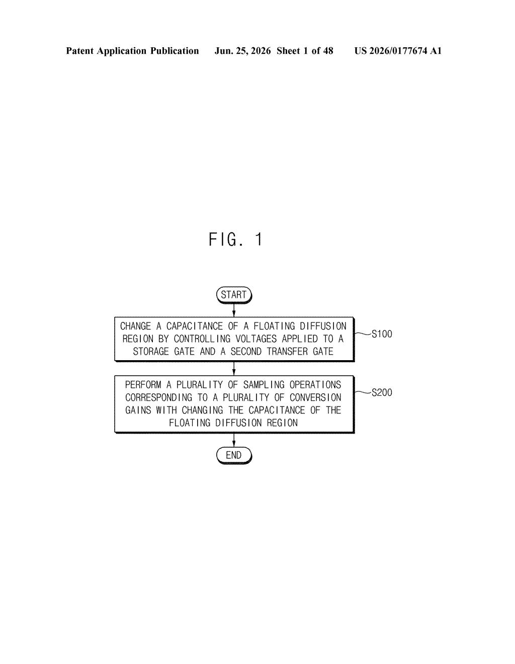
The clever part is that this switch happens inside a tiny circuit on the chip itself, by rerouting charge through different gates and changing how much electrical storage the chip uses. No moving parts, no separate sensor module, just the same pixel doing two jobs one after the other.
How the gate-switching circuit changes capacitance mid-read
Time-of-flight (ToF) sensors work by flashing infrared light and measuring how long the reflected photons take to return, letting a device calculate exact distances for things like face unlock, augmented reality, or autofocus. The core challenge is dynamic range: nearby bright surfaces flood the sensor with too many photons, while distant dark surfaces return almost none.
Samsung's patent addresses this with a pixel design that supports two conversion gains (the ratio of incoming light to output voltage signal). A high conversion gain makes the sensor very sensitive, ideal for low light. A low conversion gain handles high-brightness situations without saturating.
The pixel contains three gates in sequence between the light-collecting photodiode and the output node called the floating diffusion region:
- A first transfer gate that moves charge from the photodiode into storage
- A storage gate that holds collected charge temporarily
- A second transfer gate that controls whether extra capacitance (electrical storage) is added to the output node
For the sensitive first reading, the second transfer gate is closed, keeping the output node's capacitance small and the gain high. For the second reading, the storage gate closes and the second transfer gate opens, connecting additional capacitance to the output node and lowering the gain. The two readings are then combined to produce a depth measurement with much wider usable range than a single-gain design.
What this means for 3D cameras in phones and AR devices
For smartphones and AR headsets, accurate depth sensing in mixed lighting is one of the harder unsolved problems. A sensor that clips on bright surfaces produces wrong depth values, which means face-ID can fail, AR objects float at the wrong distance, and portrait-mode background blur cuts off in the wrong places. A chip-level fix like this one could make depth cameras more reliable across the kinds of real-world environments people actually use them in.
This is also the kind of incremental-but-important pixel-architecture work that tends to ship inside a new sensor generation rather than as a headline feature. Samsung makes image sensors for its own Galaxy phones as well as supplying chips to other manufacturers, so improvements here could ripple across a wide range of devices.
This is solid, unglamorous sensor engineering. It won't headline a product launch, but dual-conversion-gain ToF is a real limitation in current depth cameras, and a gate-level solution baked into the pixel itself is a cleaner approach than adding separate sensor arrays or doing heavy post-processing to compensate. Worth paying attention to if you follow mobile depth-sensing or AR hardware.
Get one Big Tech patent every Sunday
Plain English, intelligent commentary, no hype. Free.
Editorial commentary on a publicly published patent application. Not legal advice.