Sony Patents a Camera Chip That Switches Power Levels to Control Light Capture
Sony has filed a patent for a solid-state image sensor that can switch between two different operating voltages — a design that gives engineers more direct control over how each pixel collects and moves electric charge.
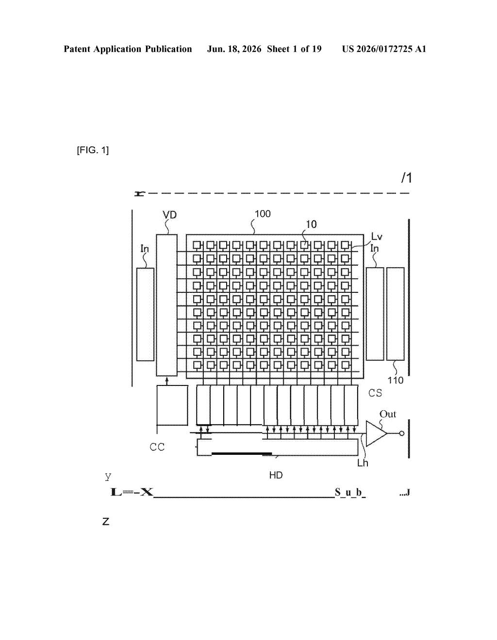
What Sony's dual-voltage image sensor actually does
Think of a camera sensor as a grid of tiny buckets, each catching light and converting it into an electrical signal. The more control you have over how those buckets fill and empty, the better your final image can be — especially in tricky lighting conditions.
Sony's patent describes a sensor pixel built in layers: a light-absorbing layer at the bottom, a charge-handling layer in the middle, and electrodes on both the top and the bottom. What makes this design notable is a circuit that can feed the pixel either of two different voltages, switching between them as needed.
By toggling between a first and second voltage, the sensor can potentially change how aggressively it gathers charge, which could help with things like reducing noise, avoiding overexposure, or adapting to different shooting conditions — all at the hardware level, before any software even gets involved.
How the pixel stack and voltage switching work together
The patent describes a solid-state imaging device — the type of chip at the heart of digital cameras and smartphone camera modules — built around a layered pixel structure and a flexible voltage supply.
Each pixel in the sensor contains:
- A photoelectric conversion layer: the part that absorbs incoming light and turns photons into electrons
- A charge accumulation/transfer layer: a middle layer that holds those electrons temporarily and then moves them onward for readout
- A charge accumulation electrode on top of that middle layer, helping control where and how charge pools
- A bottom electrode on the underside of the light-absorbing layer
The key addition is an operating voltage supply section that can selectively feed the pixel one of two distinct voltages. Think of voltage here like water pressure in a pipe — changing it alters how forcefully electrons move through the pixel structure.
Switching between the two voltage levels gives the sensor a way to change its electrical behavior on the fly. This kind of in-hardware adaptability is harder to achieve with a fixed single voltage, which is why the two-voltage architecture is the central claim of the patent.
What this could mean for Sony's camera sensor lineup
Sony's semiconductor division makes image sensors for a huge portion of the world's smartphones — including Apple's iPhones — as well as dedicated cameras, surveillance systems, and automotive cameras. Any improvement at the pixel-architecture level can ripple across millions of devices.
A sensor that can switch operating voltages at the hardware level could enable finer control over dynamic range, noise, or power consumption without relying entirely on software post-processing. That said, this patent describes a foundational structure rather than a finished product, so the real-world benefit depends entirely on how Sony implements it in an actual chip.
This is a fairly incremental sensor architecture patent — useful internal IP for Sony, but not the kind of thing that signals a dramatic new product direction. It's the sort of building-block filing that large semiconductor companies routinely accumulate to protect design flexibility in future chip generations.
Get one Big Tech patent every Sunday
Plain English, intelligent commentary, no hype. Free.
Editorial commentary on a publicly published patent application. Not legal advice.