IBM Patents a Hybrid Bonding Structure to Pull Heat Out of Stacked Chips
As chips get stacked closer together, heat has nowhere to go — and that thermal buildup is quietly becoming one of the hardest problems in modern semiconductor design. IBM's new patent proposes embedding dedicated heat-conducting channels directly through the bonding layers that hold chip stacks together.
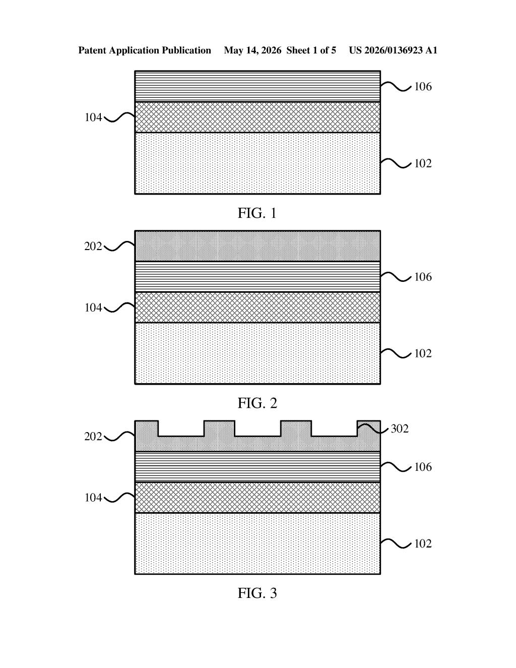
What IBM's heat-conducting channel actually does
Imagine stacking several thin pancakes on top of each other — that's roughly what modern chip stacking looks like. The problem is that heat generated in the bottom layers has a very hard time escaping through all those layers above it, causing hotspots that slow chips down or damage them over time.
IBM's patent describes a structure where a heat-conducting channel is built right into the layers that bond chips together — partially sitting in the bonding layer and partially extending into the support wafer beneath. Think of it like a copper pipe running through the floors of a building to carry heat away from the rooms.
The idea is that instead of heat slowly diffusing upward or sideways through the chip stack, it gets actively funneled through these dedicated channels into a handler wafer that can more efficiently spread and dissipate it. It's a fairly targeted structural fix for a problem that's only going to get worse as chips get denser.
How the channel spans the bonding and handler layers
The patent describes a semiconductor device built from four key stacked components:
- A device layer — where the actual transistors and active circuitry live
- A back-end-of-line (BEOL) layer — the interconnect wiring stack that sits on top of the device layer and routes electrical signals between components
- A combined bonding layer — the interface region where two chips or wafers are fused together using hybrid bonding (a technique that bonds both dielectric materials and metal pads simultaneously, enabling very tight chip-to-chip connections)
- A handler wafer — a structural support wafer that provides mechanical stability during fabrication and can serve as a thermal mass
The core innovation is a heat-conducting channel that is partially embedded in the combined bonding layer and partially embedded in the handler wafer. This means the thermal path is continuous and crosses the bonding interface — a region that traditionally acts as a thermal bottleneck because bonding materials tend to have poor thermal conductivity.
By routing a high-conductivity channel (likely a metal like copper or tungsten, though the patent doesn't limit to specific materials) through both regions simultaneously, IBM creates a low-resistance thermal pathway that moves heat away from the active device layer more efficiently than relying on bulk material conduction alone.
Why chip thermals are a real bottleneck right now
Thermal management is quietly one of the biggest constraints on advanced chip packaging — especially as AI accelerators, high-bandwidth memory stacks, and 3D-integrated chips become more common. When you stack logic and memory dies on top of each other, the heat from the bottom die has almost nowhere to go. That leads to thermal throttling, where chips automatically slow themselves down to avoid damage, eating directly into the performance you paid for.
IBM's approach targets the bonding interface specifically — which is smart, because that's often where thermal resistance is highest in a stacked structure. If this kind of channel can be reliably manufactured at scale, it could give chip designers more headroom to pack more compute into a smaller space without cooking it.
This is a solid, focused patent that addresses a real and growing engineering problem in chip packaging. It's not flashy IP — there are no AI models or UI innovations here — but thermal management in 3D chip stacks is genuinely one of the field's harder unsolved problems, and IBM's packaging research team has a credible track record in this space. Worth filing, and worth watching if you follow advanced packaging trends.
Get one Big Tech patent every Sunday
Plain English, intelligent commentary, no hype. Free.
Editorial commentary on a publicly published patent application. Not legal advice.